Beyond conventional solution-process for 2-D heterostructure
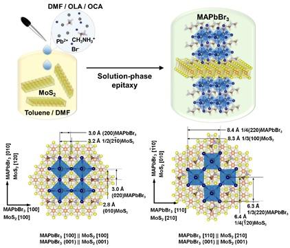
This is a schematic model of MAPbBr3||MoS2 epitaxial relationship. Credit: ©Science China Press
Xiao Huang and co-workers, who were devoted to the development for the synthesis of 2D nanomaterial-based hybrids and their applications in sensing and energy-related applications, from Nanjing Tech University, demonstrated a facile wet-chemical method to directly grow organic-inorganic hybrid perovskite (MAPbBr3, MA = CH3NH3+) NCs on surfaces of dispersible MoS2 nanosheets, recently published in Science China Materials (doi: 10.1007/s40843-018-9274-y).
Recently, TMDs and organic-inorganic hybrid perovskites have been combined into heterostructures, with the aim to marrying their good electronic and optical properties. Huang, the leader of the research group, tells us “Such heterojunctions have been realized mostly via solid-state methods typically involving chemical vapor deposition (CVD), mechanical exfoliation and/or dry transfer, which are difficult to scale-up for practical applications.”
She emphasized, “Direct growth of perovskite crystals on dispersible 2D materials in solution enables the scalable production of solution-processible hetero-structures, but has not been realized, because the precipitation of perovskite crystals usually requires a non-polar solvent, which is incompatible with most solvation conditions for 2D materials.”
By facile tuning the solvation conditions, cubic-phased MAPbBr3 (MA = CH3NH3+) nanocrystals were epitaxially deposited on trigonal/hexagonal-phased MoS2 nanosheets in solution. In spite of the mismatched lattice symmetry between the square MAPbBr3 (001) overlayer and the hexagonal MoS2 (001) substrate, two different aligning directions with lattice mismatch of as small as 1% were observed based on the domain-matching epitaxy.
This was realized most likely due to the flexible nature and absence of surface dangling bonds of MoS2 nanosheets. The formation of the epitaxial interface affords an effective energy transfer from MAPbBr3 to MoS2.
The dispersible MAPbBr3/MoS2 epitaxial heterostructures can be directly drop-casted between two graphite electrodes drawn by pencil on a piece of paper to form a photodetector with simple configuration, and demonstrated the much improved performance compared to using MoS2 or MAPbBr3 alone due to the improved light absorption and enhanced energy transfer.
In addition to the improved energy transfer and light absorption, the use of MoS2 nanosheets provided flexible and continuous substrates to connect the otherwise discrete MAPbBr3 nanocrystals and achieved the better film forming ability.
Prof. Xiao Huang tells us “The scalable preparation of heterostructures based on organic-inorganic hybrid perovskites and 2D materials via solution-phase epitaxy may bring about more opportunities for expanding their optoelectronic applications.”
###
This research was funded by the National Natural Science Foundation of China (51322202), and the Young 1000 Talents Global Recruitment Program of China.
See the article: Zhipeng Zhang, Fangfang Sun, Zhaohua Zhu, Jie Dai, Kai Gao, Qi Wei, Xiaotong Shi, Qian Sun, Yan Yan, Hai Li, Haidong Yu, Guichuan Xing, Xiao Huang, Wei Huang. “Unconventional solution-phase epitaxial growth of organic-inorganic hybrid perovskite nanocrystals on metal sulfide nanosheets.”
Sci. China Mater. 2018, doi: 10.1007/s40843-018-9274-y.
http://engine.
Media Contact
More Information:
http://dx.doi.org/10.1007/s40843-018-9274-yAll latest news from the category: Materials Sciences
Materials management deals with the research, development, manufacturing and processing of raw and industrial materials. Key aspects here are biological and medical issues, which play an increasingly important role in this field.
innovations-report offers in-depth articles related to the development and application of materials and the structure and properties of new materials.


Newest articles

Silicon Carbide Innovation Alliance to drive industrial-scale semiconductor work
Known for its ability to withstand extreme environments and high voltages, silicon carbide (SiC) is a semiconducting material made up of silicon and carbon atoms arranged into crystals that is…

New SPECT/CT technique shows impressive biomarker identification
…offers increased access for prostate cancer patients. A novel SPECT/CT acquisition method can accurately detect radiopharmaceutical biodistribution in a convenient manner for prostate cancer patients, opening the door for more…

How 3D printers can give robots a soft touch
Soft skin coverings and touch sensors have emerged as a promising feature for robots that are both safer and more intuitive for human interaction, but they are expensive and difficult…

