'Bendy' LEDs
This is a rendering of the micro-rod growth process. Credit: Seoul National University
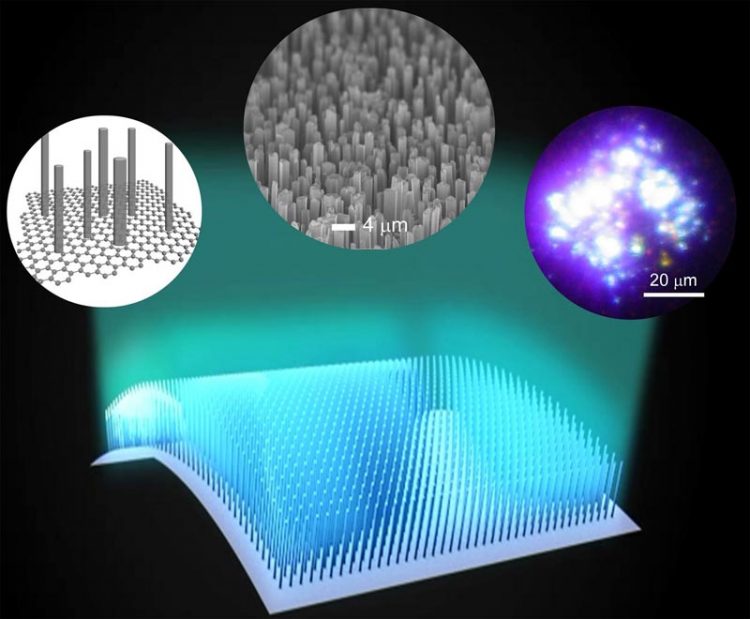
“Bendy” light-emitting diode (LED) displays and solar cells crafted with inorganic compound semiconductor micro-rods are moving one step closer to reality, thanks to graphene and the work of a team of researchers in Korea.
Currently, most flexible electronics and optoelectronics devices are fabricated using organic materials. But inorganic compound semiconductors such as gallium nitride (GaN) can provide plenty of advantages over organic materials for use in these devices — including superior optical, electrical and mechanical properties.
One major obstacle that has so far prevented the use of inorganic compound semiconductors in these types of applications was the difficulty of growing them on flexible substrates.
In the journal APL Materials, from AIP Publishing, a team of Seoul National University (SNU) researchers led by Professor Gyu-Chul Yi describes their work growing GaN micro-rods on graphene to create transferrable LEDs and enable the fabrication of bendable and stretchable devices.
“GaN microstructures and nanostructures are garnering attention within the research community as light-emitting devices because of their variable-color light emission and high-density integration properties,” explained Yi. “When combined with graphene substrates, these microstructures also show excellent tolerance for mechanical deformation.”
Why choose graphene for substrates? Ultrathin graphene films consist of weakly bonded layers of hexagonally arranged carbon atoms held together by strong covalent bonds. This makes graphene an ideal substrate “because it provides the desired flexibility with excellent mechanical strength — and it's also chemically and physically stable at temperatures in excess of 1,000°C,” said Yi.
It's important to note that for the GaN micro-rod growth, the very stable and inactive surface of graphene offers a small number of nucleation sites for GaN growth, which would enhance three-dimensional island growth of GaN micro-rods on graphene.
To create the actual GaN microstructure LEDs on the graphene substrates, the team uses a catalyst-free metal-organic chemical vapor deposition (MOCVD) process they developed back in 2002.
“Among the technique's key criteria, it's necessary to maintain high crystallinity, control over doping, formation of heterostructures and quantum structures, and vertically aligned growth onto underlying substrates,” Yi says.
When the team put the bendability and reliability of GaN micro-rod LEDs fabricated on graphene to the test, they found that “the resulting flexible LEDs showed intense electroluminescence (EL) and were reliable — there was no significant degradation in optical performance after 1,000 bending cycles,” noted Kunook Chung, the article's lead author and a graduate student in SNU's Physics Department.
This represents a tremendous breakthrough for next-generation electronics and optoelectronics devices — enabling the use of large-scale and low-cost manufacturing processes.
“By taking advantage of larger-sized graphene films, hybrid heterostructures can be used to fabricate various electronics and optoelectronics devices such as flexible and wearable LED displays for commercial use,” said Yi.
The article, “Growth and characterizations of GaN micro-rods on graphene films for flexible light-emitting diodes,” is authored by Kunook Chung, Hyeonjun Beak, Youngbin Tchoe, Hongseok Oh, Hyobin Yoo, Miyoung Kim, and Gyu-Chul Yi. It will appear in the journal APL Materials on September 23, 2014. After that date, it can be accessed at: http://scitation.aip.org/content/aip/journal/aplmater/2/9/10.1063/1.4894780
ABOUT THE JOURNAL
APL Materials is a new open access journal featuring original research on significant topical issues within the field of materials science. See: http://aplmaterials.aip.org
Media Contact
All latest news from the category: Materials Sciences
Materials management deals with the research, development, manufacturing and processing of raw and industrial materials. Key aspects here are biological and medical issues, which play an increasingly important role in this field.
innovations-report offers in-depth articles related to the development and application of materials and the structure and properties of new materials.


Newest articles

Superradiant atoms could push the boundaries of how precisely time can be measured
Superradiant atoms can help us measure time more precisely than ever. In a new study, researchers from the University of Copenhagen present a new method for measuring the time interval,…

Ion thermoelectric conversion devices for near room temperature
The electrode sheet of the thermoelectric device consists of ionic hydrogel, which is sandwiched between the electrodes to form, and the Prussian blue on the electrode undergoes a redox reaction…

Zap Energy achieves 37-million-degree temperatures in a compact device
New publication reports record electron temperatures for a small-scale, sheared-flow-stabilized Z-pinch fusion device. In the nine decades since humans first produced fusion reactions, only a few fusion technologies have demonstrated…

