A new material for solar panels could make them cheaper, more efficient
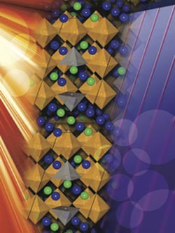
An illustration of the perovskite crystal fabricated in the experiment. Click to enlarge. Image credit: Felice Macera<br>
It also reaches a four-decade-old goal of discovering a bulk photovoltaic material that can harness energy from visible and infrared light, not just ultraviolet light.
Scaling up this new design from its tablet-size prototype to a full-size solar panel would be a large step toward making solar power affordable compared with other means of producing electricity. It would also help the nation toward its goal of creating a national power grid that receives one-third of its power through wind and solar sources.
This affordable sun-powered future could be closer than we think thanks to early tests on this new material, which was developed by a team led by scientists at the University of Pennsylvania and Drexel University. The tests were conducted, in part, at the Advanced Photon Source housed at the U.S. Department of Energy’s Argonne National Laboratory.
The team created a new class of ceramic materials that has three main benefits. First, it can produce a solar panel that is thinner than today’s silicon-based market leaders by using one material to do the work of two. Second, it uses cheaper materials than those used in today’s high-end thin-film solar panels. Third, the material is ferroelectric, which means it can switch polarity, a key trait for exceeding the theorized energy-efficiency limits of today’s solar cell material.
Part of the reason solar panels have low efficiency is that the particles collected from the sun enter the solar cell and spread out in all directions. Getting them all to flow one direction typically requires layers of different channeling material. Each time the particles pass between these layers some get lost, decreasing the energy efficiency of the solar cell. The team’s new design uses fewer layers to limit loss and uses ferroelectric material to use up less energy channeling the particles.
It took more than five years to model and design a material with this combination of properties. The material uses perovskite crystals made with a combination of potassium niobate and barium nickel niobate. It has shown significant improvement over today’s classic ferroelectric material. The new material can absorb six times more energy and transfer a photocurrent 50 times denser. Further tuning of the material’s composition should expand efficiency, the scientists say.
“This family of materials is all the more remarkable because it is comprised of inexpensive, non-toxic and earth-abundant elements, unlike compound semiconductor materials currently used in efficient thin-film solar cell technology,” said Jonathan Spanier, a team member from Drexel’s Department of Materials Science and Engineering.
The work is outlined in a paper “Perovskite oxides for visible-light-absorbing ferroelectric and photovoltaic materials” published last month in the journal Nature.
The researchers used X-ray crystallography and powder diffraction at Sector 11 of the APS to ensure the material had the crystal structure and symmetry they intended. This instrument and its unique mail-in program afford convenient and rapid access to the highest-resolution powder diffraction data available in North America, providing a very detailed and accurate picture of this ceramic material’s atomic structure.
Using a suite of experimental tools, the research team demonstrated the material’s ability to move energy in one direction without crossing layers, thus minimizing energy loss. This ability called bulk photovoltaic effect has been known since the 1970s but, until now, was only observable in ultraviolet light, and most of the energy from the sun is in the visible and infrared spectrum.
By adjusting the percentages of component elements in this new material, the research team demonstrated that they can reduce the amount of energy needed to induce conduction, a level called bandgap.
“The parent material’s bandgap is in the UV range,” Spanier said, “but adding just 10 percent of the barium nickel niobate moves the bandgap into the visible range and close to the desired value for efficient solar-energy conversion.”
The study was led by professor Andrew Rappe and research specialist Ilya Grinberg of the Department of Chemistry in Penn’s School of Arts and Sciences, along with chair Peter Davies of the Department of Materials science and Engineering in the School of Engineering and Applied Science, and Spanier from Drexel University.
Use of the APS was supported by the DOE’s Office of Science. The research was supported by the Energy Commercialization Institute of Ben Franklin Technology Partners, the Department of Energy’s Office of Basic Sciences, the Army Research Office, the American Society for Engineering Education, the Office of Naval Research and the National Science Foundation. In addition, the researchers made use of the National Energy Research Computing Center at Lawrence Berkeley National Laboratory, also supported by DOE’s Office of Science.
The Advanced Photon Source at Argonne National Laboratory is one of five national synchrotron radiation light sources supported by the U.S. Department of Energy’s Office of Science to carry out applied and basic research to understand, predict, and ultimately control matter and energy at the electronic, atomic, and molecular levels, provide the foundations for new energy technologies, and support DOE missions in energy, environment, and national security. To learn more about the Office of Science X-ray user facilities, visit the user facilities directory.
Argonne National Laboratory seeks solutions to pressing national problems in science and technology. The nation's first national laboratory, Argonne conducts leading-edge basic and applied scientific research in virtually every scientific discipline. Argonne researchers work closely with researchers from hundreds of companies, universities, and federal, state and municipal agencies to help them solve their specific problems, advance America's scientific leadership and prepare the nation for a better future. With employees from more than 60 nations, Argonne is managed by UChicago Argonne, LLC for the U.S. Department of Energy's Office of Science.
DOE’s Office of Science is the single largest supporter of basic research in the physical sciences in the United States, and is working to address some of the most pressing challenges of our time. For more information, please visit science.energy.gov.
Media Contact
More Information:
http://www.anl.govAll latest news from the category: Materials Sciences
Materials management deals with the research, development, manufacturing and processing of raw and industrial materials. Key aspects here are biological and medical issues, which play an increasingly important role in this field.
innovations-report offers in-depth articles related to the development and application of materials and the structure and properties of new materials.


Newest articles

Superradiant atoms could push the boundaries of how precisely time can be measured
Superradiant atoms can help us measure time more precisely than ever. In a new study, researchers from the University of Copenhagen present a new method for measuring the time interval,…

Ion thermoelectric conversion devices for near room temperature
The electrode sheet of the thermoelectric device consists of ionic hydrogel, which is sandwiched between the electrodes to form, and the Prussian blue on the electrode undergoes a redox reaction…

Zap Energy achieves 37-million-degree temperatures in a compact device
New publication reports record electron temperatures for a small-scale, sheared-flow-stabilized Z-pinch fusion device. In the nine decades since humans first produced fusion reactions, only a few fusion technologies have demonstrated…

