A little tension yields enormous solar crystals
In-depth analysis of the mechanisms that generate floating crystals from hot liquids could lead to large-scale, printable solar cells Credit: Reproduced with permission from reference 1© 2017 American Chemical Society
In their natural state, perovskites have difficultly moving solar-generated electricity because they crystallize with randomly oriented grains. Osman Bakr from KAUST's Solar Center and coworkers are working on ways to dramatically speed up the flow of these charge carriers using inverse temperature crystallization (ITC).
This technique uses special organic liquids and thermal energy to force perovskites to solidify into structures resembling single crystals–the optimal arrangements for device purposes.
While ITC produces high-quality perovskites far faster than conventional chemical methods, the curious mechanisms that initiate crystallization in hot organic liquids are poorly understood. Ayan Zhumekenov, a PhD student in Bakr's group, recalls spotting a key piece of evidence during efforts to adapt ITC toward large-scale manufacturing.
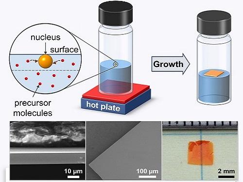
“At some point, we realized that when crystals appeared, it was usually at the solution's surface,” he says. “And this was particularly true when we used concentrated solutions.”
The KAUST team partnered with Oxford theoreticians to identify how interfaces influence perovskite growth in ITC. They propose that metal halides and solvent molecules initially cling together in tight complexes that begin to stretch and weaken at higher temperatures. With sufficient thermal energy, the complex breaks and perovskites begin to crystallize.
But interestingly, the researchers found that complexes located at the solution surface can experience additional forces due to surface tension–the strong cohesive forces that enable certain insects to stride over lakes and ponds.
The extra pull provided by the surface makes it much easier to separate the solvent-perovskite complexes and nucleate crystals that float on top of the liquid.
Exploiting this knowledge helped the team produce centimeter-sized, ultrathin single crystals and prototype a photodetector with characteristics comparable to state-of-the-art devices. Although the single crystals are currently fragile and difficult to handle due to their microscale thicknesses, Zhumekenov explains that this method could help direct the perovskite growth onto specific substrates.
“Taking into account the roles of interfaces and surface tension could have a fundamental impact,” he says, “we can get large-area growth, and it's not limited to specific metal cations–you could have a library of materials with perovskite structures.”
Media Contact
All latest news from the category: Materials Sciences
Materials management deals with the research, development, manufacturing and processing of raw and industrial materials. Key aspects here are biological and medical issues, which play an increasingly important role in this field.
innovations-report offers in-depth articles related to the development and application of materials and the structure and properties of new materials.


Newest articles

Silicon Carbide Innovation Alliance to drive industrial-scale semiconductor work
Known for its ability to withstand extreme environments and high voltages, silicon carbide (SiC) is a semiconducting material made up of silicon and carbon atoms arranged into crystals that is…

New SPECT/CT technique shows impressive biomarker identification
…offers increased access for prostate cancer patients. A novel SPECT/CT acquisition method can accurately detect radiopharmaceutical biodistribution in a convenient manner for prostate cancer patients, opening the door for more…

How 3D printers can give robots a soft touch
Soft skin coverings and touch sensors have emerged as a promising feature for robots that are both safer and more intuitive for human interaction, but they are expensive and difficult…

