Research project adopts entirely new approach to developing micro-electromechanical systems (MEMS)
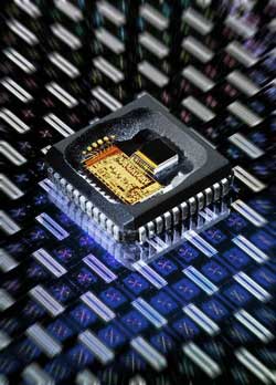
Insight of a hybrid inertial sensor package which is assembled in electronic control units (ECU).<br>Source: Robert Bosch GmbH<br>
They are working together in the research project known as “Circuit Diagram-Based Design of MEMS for Applications in Optics and Robotics” – or MEMS2015 for short.
This project is funded by the Federal Ministry of Education and Research (BMBF) and coordinated by Robert Bosch GmbH. The aim is to develop the first ever universal design methodology for MEMS to plug the gaps between electronics and mechanics design, manufacturing, and subsequent integration into products.
MEMS are tiny components that require a minimum of space to measure and electronically process parameters such as acceleration, pressure, distance, temperature, light, or chemical concentrations. With their sophisticated, compact sensor and actuator systems, MEMS can for instance be used to ensure that airbags are inflated promptly before a car is involved in a collision, to measure blood pressure or oxygen content in intensive care applications, or to enable digital cameras to eliminate camera shake.
Potential 50 percent increase in the market for MEMS
The new development methods for MEMS will allow innovative sensor and actuator systems to be developed – providing robots, for instance, with more effective sight and touch in the future. What is more, the potential market for MEMS stands to increase by up to 50 percent as a result. Using a type of modular system, the MEMS2015 researchers aim to plug the gaps between chip and sensor manufacturing on the one hand and the subsequent integration of the modules into products on the other. This will substantially increase the opportunities for widespread use of MEMS in the professional and security-relevant segments. The new methods will also allow small and medium-sized enterprises to design MEMS and integrate them into their products much more often, as well as in a wider range of configurations than at present.
Projecting images directly onto the retina
These new development methods for MEMS will pave the way for entirely new solutions in the leading-edge applications of optics and robotics. This opens up the prospect of the wide-ranging use of micromirror arrays, similar to the devices already being used in projectors. This technology allows images to be projected directly onto the retina using special glasses. In robotics, force sensors and profilometers can be developed that analyze surfaces even more accurately than before, or that simulate an extremely precise sense of touch. The project findings are being verified as part of the project on the basis of real MEMS prototypes which, in turn, serve as demonstrators.
“The project opens up innovations in mechanical engineering and process plant engineering by using powerful sensor and actuator systems based on groundbreaking MEMS and chip technologies,” says Dr. Mirco Meiners, the project coordinator for MEMS2015 who works in the Bosch Automotive Electronics division. “The clear focus of funding from Germany’s Federal Ministry of Education and Research (BMBF) helps companies maintain their lead in innovation for key technology topics and develop new innovative, complex products.”
“The MEMS2015 project raises the bar when it comes to the quality and especially the productivity of MEMS design,” says Prof. Dr. Ralf Sommer, the scientific director of the Institut für Mikroelektronik- und Mechatronik-Systeme gemeinnützige GmbH, one of the eight partners in the project. “Basic concepts such as circuit diagram-based design, which are already successfully used in microelectronics design, are now being transferred to MEMS design. This offers users enormous advantages: for one thing, MEMS2015 facilitates new highly complex products, such as micromirror arrays, and speeds up the process of bringing them to market. For another, the project will allow us in the long run to produce a Lego-brick-style design. This will above all benefit small and medium-sized enterprises, allowing them to put together their own individual, tailor-made solutions in a flexible modular MEMS and electronics system.”
Eight partners from research and industry
The MEMS2015 research project, which has a three-year term and around 3.5 million euros in funding from Germany’s Federal Ministry of Education and Research (BMBF) as part of the German government’s High-Tech Strategy and the ICT 2020 development program, brings together the potential of eight partners from research and industry: Cadence Design Systems GmbH, Carl Zeiss SMT GmbH, Institut für Mikroelektronik- und Mechatronik-Systeme GmbH, Robert Bosch GmbH, the Technical University of Munich, TETRA Gesellschaft für Sensorik, Robotik und Automation mbH, the University of Bremen, and X-FAB Semiconductor Foundries AG. The edacentrum in Hannover is responsible for project management for MEMS2015.
For more information, visit http://www.edacentrum.de/mems2015
Press Contact:
Ralf Popp, edacentrum, Phone: +49 (511) 762-19697, Fax: +49 (511) 762-19695, popp@edacentrum.de
About edacentrum
The edacentrum is an independent institution dedicated to the promotion of research and development in the area of electronic design automation (EDA). Founded by the German microelectronics industry, it was funded during its early years by the German Federal Ministry of Education and Research (BMBF). The primary role of edacentrum is to initiate, evaluate and supervise industry-driven R&D projects, and to offer a comprehensive spectrum of services to support all matters concerning EDA development. Moreover, by encouraging EDA cluster research projects and EDA networks and by providing a communication platform for the EDA community, edacentrum brings together and reinforces the EDA expertise of universities and research institutes. The edacentrum seeks to increase awareness among upper management, the public and the political arena, of the critical importance of design automation for solving complex system and semiconductor problems, especially those associated with micro- and nanoelectronics.
Media Contact
All latest news from the category: Power and Electrical Engineering
This topic covers issues related to energy generation, conversion, transportation and consumption and how the industry is addressing the challenge of energy efficiency in general.
innovations-report provides in-depth and informative reports and articles on subjects ranging from wind energy, fuel cell technology, solar energy, geothermal energy, petroleum, gas, nuclear engineering, alternative energy and energy efficiency to fusion, hydrogen and superconductor technologies.


Newest articles

Silicon Carbide Innovation Alliance to drive industrial-scale semiconductor work
Known for its ability to withstand extreme environments and high voltages, silicon carbide (SiC) is a semiconducting material made up of silicon and carbon atoms arranged into crystals that is…

New SPECT/CT technique shows impressive biomarker identification
…offers increased access for prostate cancer patients. A novel SPECT/CT acquisition method can accurately detect radiopharmaceutical biodistribution in a convenient manner for prostate cancer patients, opening the door for more…

How 3D printers can give robots a soft touch
Soft skin coverings and touch sensors have emerged as a promising feature for robots that are both safer and more intuitive for human interaction, but they are expensive and difficult…

