Develop data glasses faster
Ultra-low power OLED microdisplay © Fraunhofer FEP, picture in printable resolution: www.fep.fraunhofer.de/press
Augmented Reality (AR) and Virtual Reality (VR) are technologies that are increasingly being integrated in both our private and working lives. The number of data glasses being marketed is growing rapidly because the required technologies have now reached a level that makes compact, capable, and comfortable data glasses feasible.
Scientists at Fraunhofer FEP have specialized in the development of custom microdisplays for AR and VR data glasses. “We utilize OLED-on-silicon technology for our microdisplays. OLEDs are self-illuminating, requiring no additional illumination in comparison to other types of displays, and therefore facilitate simplified optics and considerably higher contrast ratios”, explains Bernd Richter, deputy head of the Microdisplays and Sensors Division at Fraunhofer FEP. “Additional functionality can even be directly integrated into the display, such as a microminiature camera for controlling the information displayed in glasses using eye tracking.”
The way that data glasses are designed and constructed is as varied as their application areas – such as assisted equipment maintenance, in health examinations, or as a simple display of information for joggers and cyclists.
To make the developer’s job of incorporating OLED-on-silicon technology the most suitable way as easy as possible, the scientists offer evaluation kits for use as development tools.
Controlling content with eye tracking
One specialized configuration is a bidirectional microdisplay that combines a high-resolution SVGA OLED microdisplay and an embedded SVGA image sensor in a single region of an active device. With these evaluation kits glasses can be developed that make it possible to use the eyes to control what content is displayed, thereby freeing up the hands for assembly work, for example. Moreover, these bidirectional displays can be used as the basis for developing and evaluating optical sensors such as optical finger print sensors, for example.
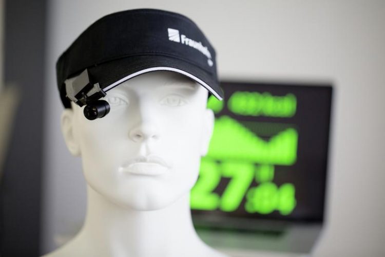
Ultra-low power OLED microdisplays
Ultra-low-power displays are especially suitable for displaying simple information. Though they have limited resolution, they nevertheless can reduce the current consumption to a small fraction through an innovative approach in the design of the display backplane as well as advanced system design. This facilitates considerably longer operating times for batteries and also delivers more compact, lighter systems. The approach is particularly advantageous for data glasses used to display navigation or fitness data by athletes.
Large-area OLED microdisplays
An evaluation kit with an especially large-scale OLED microdisplay that is primarily of interest for VR applications will be presented for the first time at embedded world 2018. This OLED microdisplay was developed in the LOMID project (Large-area costefficient OLED microdisplays and their application, www.lomid.eu). This project has received funding from the European Union’s Horizon 2020 research and innovation programme under grant agreement No. 644101.
The scientists are also ready of course to develop client-specific OLED microdisplays that are adapted to perfectly fit the purpose of the display. OLED-on-silicon technology is likewise being employed for sensors: such as for any sensing job that has to rely on something being initially illuminated, then detecting and evaluating the reflected light in real time – such as in optical sensors for biological sensing applications and finger print sensors.
Press contact:
Mrs. Annett Arnold
Fraunhofer Institute for Organic Electronics, Electron Beam and Plasma Technology FEP
Phone +49 351 2586 333 | presse@fep.fraunhofer.de
Winterbergstraße 28 | 01277 Dresden | Germany | www.fep.fraunhofer.de
Media Contact
All latest news from the category: Trade Fair News


Newest articles

Silicon Carbide Innovation Alliance to drive industrial-scale semiconductor work
Known for its ability to withstand extreme environments and high voltages, silicon carbide (SiC) is a semiconducting material made up of silicon and carbon atoms arranged into crystals that is…

New SPECT/CT technique shows impressive biomarker identification
…offers increased access for prostate cancer patients. A novel SPECT/CT acquisition method can accurately detect radiopharmaceutical biodistribution in a convenient manner for prostate cancer patients, opening the door for more…

How 3D printers can give robots a soft touch
Soft skin coverings and touch sensors have emerged as a promising feature for robots that are both safer and more intuitive for human interaction, but they are expensive and difficult…

