International Conference on Design and Technology in the IC Industry
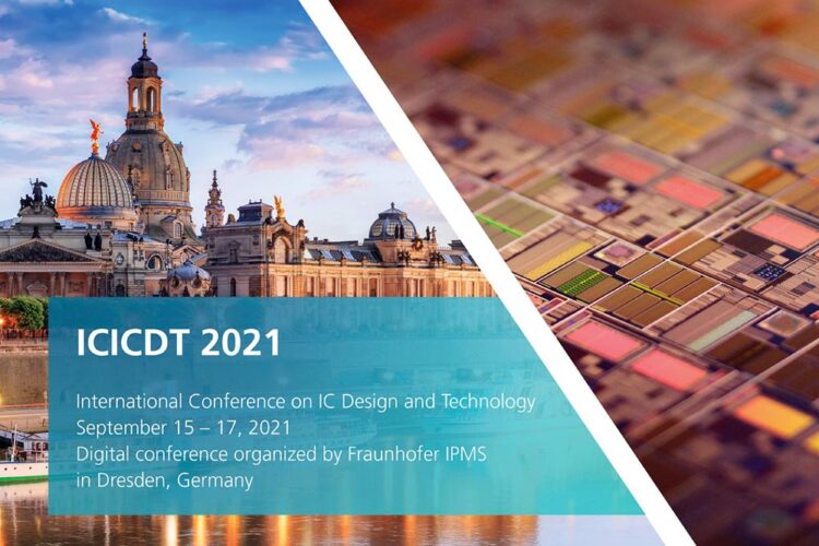
International Conference on Design and Technology in the IC Industry
(c) Fraunhofer IPMS
Today, the mutual optimization of design and technology provide key advantage in the highly competitive semiconductor market. Traditionally, when developing integrated circuits (IC), their design and technology were considered and developed separately. Looking to the future, this is no longer appropriate. Experienced IC designers need a deeper understanding of the interactions between design and technology options to ensure maximum product optimization.
For the 18th time, the “International Conference on IC Design and Technology (ICICDT)” provides a forum for engineers, researchers, graduate students and professors to cross the boundary between design and technology.
The trend in the IC industry is toward specialized system designs and manufacturing outsourcing, such as fabless design house and wafer foundries. This also increases the need for individuals with multidisciplinary technical skills for cross-sector collaboration. In addition, advanced IC technology no longer provides the same level of control over many parameters that negatively impact circuit behavior. At the same time, today’s IC designs are reaching technological limits and in some cases require special fine-tuning of specific process modules in manufacturing. As a result, the traditionally separate areas of design and technology are increasingly intertwined.
Close, multidisciplinary collaboration in the semiconductor industry favors the implementation of new designs and new technologies. This allows products to be optimized for higher performance as well as lower energy consumption and accelerates their time-to-market. To break down the traditional boundaries between design and technology, the ICICDT conference was launched in 2004. It provides an important international forum for interaction and collaboration of IC design and technology and is sponsored by the Institute of Electrical and Electronics Engineers (IEEE).
The organizer of this year’s ICICDT, which will be held in virtual format from September 15 to 17, is the Fraunhofer Institute for Photonic Microsystems IPMS in Dresden, Germany. “We are proud to host this year’s ICICDT,” says Fraunhofer IPMS deputy institute director and conference co-chair Dr. Wenke Weinreich. “Even though we cannot welcome our international guests in person due to the pandemic situation, participants can expect inspiring lectures and workshops that offer plenty of room for interaction and exchange.” Engineers, researchers, scientists, professors and students will be offered a platform to cross the boundary between design and process technology in product development and manufacturing.
“The unique workshop style of the conference offers technologists and product designers the opportunity to share breakthrough ideas and collaborate effectively,” continues Dr. Wenke Weinreich. The one-day tutorial program on plasma-induced damage, GaN power devices, neuromorphic computing for edge AI, and large-scale silicon photonic MEMS switches will be followed by two days of technical presentations and workshops. “This will cover topics that require close interaction and collaboration through all fields of design, device, and process to achieve improvement in product development and manufacturing.” Examples include optimizations in problematic leakage currents, energy efficiency, noise issues in mixed signals, large scale IC devices, process- and plasma-induced damage, or device and process parameter fluctuation. The incorporation of new materials or the implementation of new technologies, such as PDSOI, FDSOI or MRAM, will also be addressed in the conference.
“We are excited about the unique format of this year’s ICICDT as a virtual event. A recorded short presentation will be available for each talk, there will be live workshops, Q&As, networking and an entertaining social program. The latter includes a virtual city tour to introduce our location in the beautiful city of Dresden,” concludes Dr. Wenke Weinreich.
About Fraunhofer IPMS
The Fraunhofer Institute for Photonic Microsystems IPMS stands for applied research and development in the fields of intelligent industrial solutions, medical technology and improved quality of life. Our research focuses on miniaturized sensors and actuators, integrated circuits, wireless and wired data communication, and customized MEMS systems.
With the Center Nanoelectronic Technologies (CNT), Fraunhofer IPMS contributes applied research on 300 mm wafers for microchip producers, suppliers, equipment manufacturers and R&D partners.
Media Contact
All latest news from the category: Event News
Newest articles

Bringing bio-inspired robots to life
Nebraska researcher Eric Markvicka gets NSF CAREER Award to pursue manufacture of novel materials for soft robotics and stretchable electronics. Engineers are increasingly eager to develop robots that mimic the…

Bella moths use poison to attract mates
Scientists are closer to finding out how. Pyrrolizidine alkaloids are as bitter and toxic as they are hard to pronounce. They’re produced by several different types of plants and are…

AI tool creates ‘synthetic’ images of cells
…for enhanced microscopy analysis. Observing individual cells through microscopes can reveal a range of important cell biological phenomena that frequently play a role in human diseases, but the process of…


