Hannover Messe: Inkjet process to cost-efficiently print flexible touchscreens
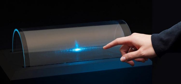
Flexible touchscreens with inkjetprinting. Source: INM; free within this press release
INM will be demonstrating flexible touch screens, which are produced by printing recently developed nanoparticle inks on thin plastic foils. These inks composed predominantly of transparent, conductive oxides (TCOs) are suitable for a one-step printing process.
The transparent lines and patterns are obtained by inkjet printing or alternatively by direct gravure printing, which are electrically conductive even after bending. Thus, a one-step-printing process for cost-efficient electrode patterns is enabled.
Conductive coatings with TCOs are usually applied by means of high vacuum techniques such as sputtering. For patterning of the TCO coatings additional cost-intensive process steps are necessary, for example photolithography and etching.
“We produce TCO nanoparticles with special surface properties,” explains Peter William de Oliveira, Head of the Optical Materials Program Division. “The TCO ink is then created by adding a solvent and a special binder to these TCO particles. The binder performs several tasks here: it not only makes the TCO nanoparticles adhere well on the substrate; but it also increases the flexibility of the TCO coating: in this way, the conductivity is maintained even when the films are bent. Using an adapted electrode pattern, flexible capacitive touch screen sensors with high sensitivity and resolution is printed in a simple process”.
After curing under UV light at low temperatures less than 130 degrees centigrade, the touch screen is completed.
Transparent, electronically conductive inks allow conductor tracks to be produced easily even on classic reel-to-reel processes. Initial trials at INM have been promising. The researchers all agree that in the future the use of structured rollers will allow structured, conductive surfaces to be printed with a high throughput at low cost.
Your expert at INM
Dr. Peter William de Oliveira
INM – Leibniz Institute for New Materials
Head Optical Materials
Head InnovationCenter INM
Phone: +49681-9300-148
OptiMat@leibniz-inm.de
INM – Leibniz Institute for New Materials, situated in Saarbrücken, is an internationally leading centre for materials research. INM conducts research and development to create new materials – for today, tomorrow and beyond. Research at INM is performed in three fields: Nanocomposite Technology, Interface Materials, and Bio Interfaces. INM is an institute of the Leibniz Association and has about 240 employees.
Media Contact
All latest news from the category: Trade Fair News


Newest articles

Properties of new materials for microchips
… can now be measured well. Reseachers of Delft University of Technology demonstrated measuring performance properties of ultrathin silicon membranes. Making ever smaller and more powerful chips requires new ultrathin…

Floating solar’s potential
… to support sustainable development by addressing climate, water, and energy goals holistically. A new study published this week in Nature Energy raises the potential for floating solar photovoltaics (FPV)…

Skyrmions move at record speeds
… a step towards the computing of the future. An international research team led by scientists from the CNRS1 has discovered that the magnetic nanobubbles2 known as skyrmions can be…

