HiVP-CMOS (High Voltage-High Power-CMOS)

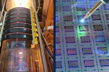
A novel arrangement, namely cascading with “resistive diode boosting”, makes it possible to increase the output voltage of MOS power amplifiers. The invention limits the break down voltage by means of a limiting path between gate and drain. This path has a defined resistance and can be switched on or off. Additionally, it is possible to adopt a parallel configuration for high current applications
Further Information: PDF
Technologie-Lizenz-Büro (TLB) der Baden-Württembergischen Hochschulen GmbH
Phone: +49 (0)721/79 00 40
Contact
Professor Dr. Arno Basedow
Media Contact
All latest news from the category: Technology Offerings
Newest articles

Silicon Carbide Innovation Alliance to drive industrial-scale semiconductor work
Known for its ability to withstand extreme environments and high voltages, silicon carbide (SiC) is a semiconducting material made up of silicon and carbon atoms arranged into crystals that is…

New SPECT/CT technique shows impressive biomarker identification
…offers increased access for prostate cancer patients. A novel SPECT/CT acquisition method can accurately detect radiopharmaceutical biodistribution in a convenient manner for prostate cancer patients, opening the door for more…

How 3D printers can give robots a soft touch
Soft skin coverings and touch sensors have emerged as a promising feature for robots that are both safer and more intuitive for human interaction, but they are expensive and difficult…


