Galliumnitrit-Halbleiter
The invention relates to a method to wax of gallium nitride
semiconductor material on a sapphire substrate. The substrate can serve for the production of electronic components or as substrate for the epitaxy of other layers. The method of the invention is easy to realize and suited for the industrial application. It further assures the production of highquality GaN layers.
Further Information: PDF
PVA Mecklenburg-Vorpommern AG
Phone: +49 (0)381/49 74 74 0
Contact
Moritz v. Grotthuss, Dr. Rüdiger Werp
Media Contact
All latest news from the category: Technology Offerings
Newest articles
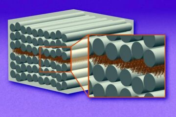
“Nanostitches” enable lighter and tougher composite materials
In research that may lead to next-generation airplanes and spacecraft, MIT engineers used carbon nanotubes to prevent cracking in multilayered composites. To save on fuel and reduce aircraft emissions, engineers…

Trash to treasure
Researchers turn metal waste into catalyst for hydrogen. Scientists have found a way to transform metal waste into a highly efficient catalyst to make hydrogen from water, a discovery that…
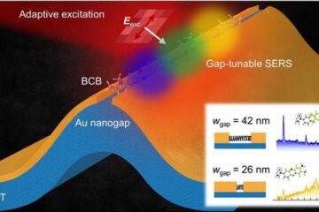
Real-time detection of infectious disease viruses
… by searching for molecular fingerprinting. A research team consisting of Professor Kyoung-Duck Park and Taeyoung Moon and Huitae Joo, PhD candidates, from the Department of Physics at Pohang University…

