Researchers demonstrate highly directional terahertz laser rays

A collaborative team of applied scientists from Harvard University and the University of Leeds have demonstrated a new terahertz (THz) semiconductor laser that emits beams with a much smaller divergence than conventional THz laser sources. The advance, published in the August 8th issue of Nature Materials, opens the door to a wide range of applications in terahertz science and technology. Harvard has filed a broad patent on the invention.
The finding was spearheaded by postdoctoral fellow Nanfang Yu and Federico Capasso, Robert L. Wallace Professor of Applied Physics and Vinton Hayes Senior Research Fellow in Electrical Engineering, both of Harvard's School of Engineering and Applied Sciences (SEAS), and by a team led by Edmund Linfield at the School of Electronic and Electrical Engineering, University of Leeds.
Terahertz rays (T-rays) can penetrate efficiently through paper, clothing, plastic, and many other materials, making them ideal for detecting concealed weapons and biological agents, imaging tumors without harmful side effects, and spotting defects, such as cracks, within materials. THz radiation is also used for high-sensitivity detection of tiny concentrations of interstellar chemicals.
“Unfortunately, present THz semiconductor lasers are not suitable for many of these applications because their beam is widely divergent—similar to how light is emitted from a lamp” says Capasso. “By creating an artificial optical structure on the facet of the laser, we were able to generate highly collimated (i.e., tightly bound) rays from the device. This leads to the efficient collection and high concentration of power without the need for conventional, expensive, and bulky lenses.”
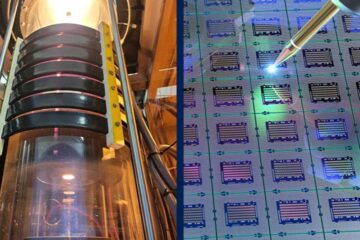
Specifically, to get around the conventional limitations, the researchers sculpted an array of sub-wavelength-wide grooves, dubbed a metamaterial, directly on the facet of quantum cascade lasers. The devices emit at a frequency of 3 THz (or a wavelength of one hundred microns), in the invisible part of the spectrum known as the far-infrared.
“Our team was able to reduce the divergence angle of the beam emerging from these semiconductor lasers dramatically, whilst maintaining the high output optical power of identical unpatterned devices,” says Linfield. “This type of laser could be used by customs officials to detect illicit substances and by pharmaceutical manufacturers to check the quality of drugs being produced and stored.”
The use of metamaterials, artificial materials engineered to provide properties which may not be readily available in Nature, was critical to the researchers' successful demonstration. While metamaterials have potential use in novel applications such as cloaking, negative refraction and high resolution imaging, their use in semiconductor devices has been very limited to date.
“In our case, the metamaterial serves a dual function: strongly confining the THz light emerging from the device to the laser facet and collimating the beam,” explains Yu. “The ability of metamaterials to confine strongly THz waves to surfaces makes it possible to manipulate them efficiently for applications such as sensing and THz optical circuits.”
Additional co-authors of the study included Qi Jie Wang, formerly of Harvard University and now with the Nanyang Technological University in Singapore; graduate student Mikhail A. Kats and postdoctoral fellow Jonathan A. Fan, both of Harvard University; and postdoctoral fellows Suraj P. Khanna and Lianhe Li and faculty member A. Giles Davies, all from the University of Leeds.
The research was partially supported by the Air Force Office of Scientific Research. The Harvard-based authors also acknowledge the support of the Center for Nanoscale Systems (CNS) at Harvard University, a member of the National Nanotechnology Infrastructure Network (NNIN). The Leeds-based authors acknowledge support from the UK's Engineering and Physical Sciences Research Council.
Quantum Cascade Lasers were first invented and demonstrated by Federico Capasso and his team at Bell Labs in 1994. At the shorter wavelengths of the mid-infrared spectrum these compact millimeter length semiconductor lasers operate routinely at room temperature with high optical powers and are a rapidly growing commercial sector for a wide range of military and civilian applications including infrared countermeasures and chemical sensing. They are made by stacking ultra-thin atomic layers of semiconductor materials on top of each other. By varying the thickness of the layers one can design the energy levels in the structure to create an artificial laser medium.
Media Contact
More Information:
http://www.seas.harvard.eduAll latest news from the category: Process Engineering
This special field revolves around processes for modifying material properties (milling, cooling), composition (filtration, distillation) and type (oxidation, hydration).
Valuable information is available on a broad range of technologies including material separation, laser processes, measuring techniques and robot engineering in addition to testing methods and coating and materials analysis processes.
Newest articles

Silicon Carbide Innovation Alliance to drive industrial-scale semiconductor work
Known for its ability to withstand extreme environments and high voltages, silicon carbide (SiC) is a semiconducting material made up of silicon and carbon atoms arranged into crystals that is…

New SPECT/CT technique shows impressive biomarker identification
…offers increased access for prostate cancer patients. A novel SPECT/CT acquisition method can accurately detect radiopharmaceutical biodistribution in a convenient manner for prostate cancer patients, opening the door for more…

How 3D printers can give robots a soft touch
Soft skin coverings and touch sensors have emerged as a promising feature for robots that are both safer and more intuitive for human interaction, but they are expensive and difficult…


