Scaling Friction Down to the Nano/Micro Realm
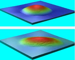
Three-dimensional images showing the topography of both round and elliptical tips used in making friction measurements
An improved method for correcting nano- and micro-scale friction measurements has been developed by researchers at the National Institute of Standards and Technology (NIST). The new technique should help designers produce more durable micro- and nano-devices with moving parts, such as tiny motors, positioning devices or encoders.
Friction measurements made at the micro- and nano-scale can differ substantially due to changes in applied load. In a series of experiments described by nanotribologist Stephen Hsu at a technical meeting held May 17-20 in Toronto,* NIST scientists confirmed that many of the measured differences appear to be caused by unintended scratching of the surface by the sharp tips used in making the measurements themselves.
The NIST team used a specially designed friction tester developed jointly by NIST and Hysitron Inc. of Minneapolis. A carefully calibrated force was applied to diamond tips having a range of sizes. Friction forces were then measured as each tip was slid across a very smooth surface of silicon. Friction at the macroscopic scale is usually straightforward—doubling the force between two objects produces twice the friction. However, work at NIST and elsewhere has shown that friction at the microscale does not always obey this scaling rule. Forces greater than about 2 milliNewton** produced substantially greater friction values than expected.
Images of the test surface made with an atomic force microscope confirmed that unintentional scratching produced the extra friction. To correct for this effect, NIST researchers developed a way to measure precisely the size, shape and orientation of the diamond tips so that friction forces caused by “plowing” can be subtracted to produce a more accurate final measurement.
Media Contact
More Information:
http://www.nist.gov/public_affairs/techbeat/tb2004_0524.htmAll latest news from the category: Process Engineering
This special field revolves around processes for modifying material properties (milling, cooling), composition (filtration, distillation) and type (oxidation, hydration).
Valuable information is available on a broad range of technologies including material separation, laser processes, measuring techniques and robot engineering in addition to testing methods and coating and materials analysis processes.


Newest articles

Silicon Carbide Innovation Alliance to drive industrial-scale semiconductor work
Known for its ability to withstand extreme environments and high voltages, silicon carbide (SiC) is a semiconducting material made up of silicon and carbon atoms arranged into crystals that is…

New SPECT/CT technique shows impressive biomarker identification
…offers increased access for prostate cancer patients. A novel SPECT/CT acquisition method can accurately detect radiopharmaceutical biodistribution in a convenient manner for prostate cancer patients, opening the door for more…

How 3D printers can give robots a soft touch
Soft skin coverings and touch sensors have emerged as a promising feature for robots that are both safer and more intuitive for human interaction, but they are expensive and difficult…

