Cost-saving Laser-based Process for Manufacturing Free-form Optics
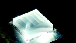
High speed laser ablation of fused silica. Fraunhofer Institute for Laser Technology ILT, Aachen<br>
The Fraunhofer Institute for Laser Technology ILT has developed a process for manufacturing optical glass components, which should be particularly suitable for the cost-effective production of aspheres and free-form optics. With this procedure, engineers will be able to produce nearly every surface geometry imaginable in the future.
In optical systems such as headlights, projectors, camera lenses and lenses for glasses, optics ensure that light is focused as well as significantly determining image quality due to their surface form and finish quality. With commonly used spherical optics, the risk of aberration typically is reduced through combining several optics in a single optical system. However, this approach also increases the weight and size of the optical system. By using non-spherical lenses, whose surface form deviates from the spherical curvature of a spherical lens, engineers can effectively minimize such aberrations. This way, two or more conventional spherical optics can be replaced by one asphere and enable higher luminous efficacy. In addition, the dimensions and the weight of the overall optical system can be reduced.
Until now, small quantities of non-spherical optics have been produced through a number of expensive and time-consuming grinding and polishing steps. While the blank pressing of optics represents one possible alternative, it, however, is only economical for larger quantities. A young research team at the Fraunhofer ILT has developed a new process for individual manufacturing of apheres and free-form optics within the scope of the project “Forming and Polishing of Optical Glass Components by Ablation and Remelting with Laser Radiation” (or FoPoLas).
Ablating, Polishing, Correcting
Sebastian Heidrich and his team have been able to produce non-spherical and free-form surfaces with different degrees of curvature out of a quadratic piece of fused silica. In order to do this, they have combined different processing techniques into one process chain: Firstly, a CO2 laser beam heats the material to over 2,230°C, the evaporation temperature of fused silica. This way, the unnecessary material is evaporated selectively and ablated. According to computer generated data, nearly any surface form desired can be produced. In a following step, CO2 laser radiation heats the surface of the component again to near the evaporation temperature so that the viscosity of the uppermost material layer is changed. It becomes fluid and its roughness is reduced on account of the surface tension. The material remains polished once it has cooled. After this laser polishing step, remaining form defects shall be corrected with laser-based precision ablation in the future.
High Economy also for Small Series Production
This process chain is directed primarily at manufacturers of individualized, non-spherical optics. Since the desired surface form is produced based on computer data, it can be changed without extensive retooling. In comparison to conventional manufacturing methods, the use of this process chain could shorten the time it takes to produce optical glass components presumably by a factor of ten. For complex free-form surfaces, this factor can even be much higher. This would mean an enormous reduction in costs and high flexibility for the production of small to medium lot sizes. The process steps can also be used separately, for example, to polish the inside of drill holes, starting from a diameter of several millimeters.
Currently the scientists are optimizing the individual steps of the process chain. Before the process can be applied in the industry, the precision of the ablation process and the surface quality of the polishing process have to be increased. In addition, an appropriate measurement technology has to be developed for form detection, in order to attain suitable optical quality of the manufactured glass components.
On May 11, experts will be presenting the process within the scope of the International Laser Technology Fair AKL’12 in the laser plant park of the Fraunhofer ILT. Interested parties can find further information on this at: www.lasercongress.org.
Contacts at the Fraunhofer ILT
Dipl.-Ing. Sebastian Heidrich
Polishing
Telephone +49 241 8906-645
sebastian.heidrich@ilt.fraunhofer.de
Dr. Edgar Willenborg
Polishing
Telephone +49 241 8906-213
edgar.willenborg@ilt.fraunhofer.de
Fraunhofer Institute for Laser Technology ILT
Steinbachstraße 15
52074 Aachen, Germany
Telephone +49 241 8906-0
Fax +49 241 8906-121
Media Contact
More Information:
http://www.ilt.fraunhofer.deAll latest news from the category: Process Engineering
This special field revolves around processes for modifying material properties (milling, cooling), composition (filtration, distillation) and type (oxidation, hydration).
Valuable information is available on a broad range of technologies including material separation, laser processes, measuring techniques and robot engineering in addition to testing methods and coating and materials analysis processes.


Newest articles

Properties of new materials for microchips
… can now be measured well. Reseachers of Delft University of Technology demonstrated measuring performance properties of ultrathin silicon membranes. Making ever smaller and more powerful chips requires new ultrathin…

Floating solar’s potential
… to support sustainable development by addressing climate, water, and energy goals holistically. A new study published this week in Nature Energy raises the potential for floating solar photovoltaics (FPV)…

Skyrmions move at record speeds
… a step towards the computing of the future. An international research team led by scientists from the CNRS1 has discovered that the magnetic nanobubbles2 known as skyrmions can be…

