Imaging 'gridlock' in high-temperature superconductors
In a standard scanning tunneling microscope (STM) topographic image of the surface of a cuprate semiconductor (left) atoms are arranged neatly in a crystal lattice (the occasional crosses represent atoms missing from the surface). At right is an image based in the ratio of up and down current flow through the STM tip showing in yellow the probable locations of “holes” where electrons are missing from the crystal structure. Short yellow bars are aligned with copper-oxygen-copper bonds, and Cornell researchers say it is significant that these areas are distributed in random locations and directions. In some cases the arrangement is a unidirectional four crystal-lattice-spacing wide domain, or “nanostripe.”
A possible explanation why is offered by new research at Cornell University. The research, reported March 5 at the annual meeting of the American Physical Society in Denver, concerns certain copper oxides — known as cuprates — that can become high-temperature superconductors, but also can, in a slightly different configuration, become stalled by the “gridlock.”
Understanding how and why that transition takes place is a crucial question for cuprate superconductivity research because, if it did not, the maximum temperatures for superconductivity could conceivably be much higher.
Scanning lightly hole-doped cuprate crystals with a highly precise scanning tunneling microscope (STM) has revealed strong variations in electronic structure with some copper-oxygen-copper (Cu-O-Cu) bonds distributed randomly through the crystal apparently exhibiting “holes” where electrons are missing. The researchers also found larger rectangular regions with missing electrons that were spaced four units of the crystal lattice apart, and may represent the first direct observation of long-sought electronic “stripes” in cuprates.
Yuhki Kohsaka, a postdoctoral researcher working with J.C. Séamus Davis, Cornell professor of physics, reported on the research. A paper on the work by Kohsaka, Davis and others is the cover story in the March 9 edition of Science.
The superconducting phenomenon was first discovered in metals cooled to less than about 4 degrees Celsius above absolute zero (-273 degrees Celsius or -459 degrees Fahrenheit) with liquid helium. Recently, superconductivity at much higher temperatures was discovered in cuprates. Pure cuprates are normally insulators, but when doped with small numbers of other atoms they become superconductors at temperatures as high as 148 degrees above absolute zero (-125 Celsius). The impurities break up the orderly crystal structure and create “holes” where electrons ought to be.
At 16 percent hole-density the cuprates display the highest temperature superconductivity of any known material. But if hole-density is reduced by just a few percent, the superconductivity vanishes precipitously and the materials become highly resistant.
Previous experiments have given evidence that long-range patterns of “stripes” of alternating high- and low-charge density, spaced four units of the crystal lattice apart, exist in doped cuprates, but no imaging technique had been able to detect them.
An STM uses an atom-sized tip that moves in atom-sized steps across a surface. When a voltage is applied between the tip and the surface, a small current known as a “tunneling current” flows between them. By adjusting the height of the tip above the surface to produce a constant current, researchers can see the shapes of individual atoms. And with the exceptional precision of the STM operated by Davis and colleagues at Cornell, the spatial arrangement of electronic states can be imaged. However, the researchers explain in their paper, this technique has serious limitations in imaging the distribution of holes.
The innovation in the new research, based on a suggestion by Nobel laureate Philip W. Anderson, professor emeritus at Princeton University, is to compare current flow in opposite directions at each point in the scan. In simple terms, at regions of the crystal containing fewer electrons (more holes), more electrons can flow down from the tip into these voids than up. The process is called TA-imaging, for tunneling asymmetry.
The Cornell researchers studied cuprate crystals in which about 10 percent of the electrons in the crystal lattice were removed and replaced by holes. The researchers imaged two cuprates with very different chemistry, crystal structure and doping characteristics and found virtually identical results, which they attribute entirely to the spatial arrangement of electrons in the crystal. The areas where TA-imaging suggests that there are holes appear to be centered on oxygen atoms within the Cu-O-Cu bond. This is what has long been expected based on X-ray scattering studies. But “the big surprise,” Davis said, “is that when you map this stuff for large distances across the surface no orderly patterns are observed. We had no picture of this before.” Perhaps even more exciting, he said, is the discovery that over larger areas the holes do appear to be arranged in patterns that are rectangular and exactly four crystal lattice spaces wide. These so called “nanostripes” are aligned with the crystal lattice but otherwise distributed at random.
“It's plausible that when you increase the number of holes these 'nanostripes' will combine into the orderly stripes seen in other experiments,” Davis said. A next step, he said, is to use TA-imaging on more heavily doped materials that exhibit such stripes to see if they are made up of these oxygen-centered holes. But the key challenge, he added, is to understand precisely how the process of hole localization into the patterns seen here suppresses superconductivity.
Co-authors of the paper include graduate students Curry Taylor, Kazuhiro Fujita and Andrew Schmidt of the Laboratory of Atomic and Solid State Physics at Cornell. The Cornell researchers worked in collaboration with scientists at the Université de Sherbrooke, Canada, the Universities of Tokyo and Kyoto and the National Institute of Advanced Industrial Science and Technology in Japan.
Media Contact
More Information:
http://www.cornell.eduAll latest news from the category: Physics and Astronomy
This area deals with the fundamental laws and building blocks of nature and how they interact, the properties and the behavior of matter, and research into space and time and their structures.
innovations-report provides in-depth reports and articles on subjects such as astrophysics, laser technologies, nuclear, quantum, particle and solid-state physics, nanotechnologies, planetary research and findings (Mars, Venus) and developments related to the Hubble Telescope.


Newest articles
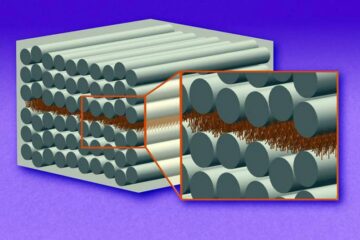
“Nanostitches” enable lighter and tougher composite materials
In research that may lead to next-generation airplanes and spacecraft, MIT engineers used carbon nanotubes to prevent cracking in multilayered composites. To save on fuel and reduce aircraft emissions, engineers…
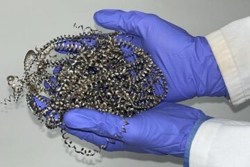
Trash to treasure
Researchers turn metal waste into catalyst for hydrogen. Scientists have found a way to transform metal waste into a highly efficient catalyst to make hydrogen from water, a discovery that…
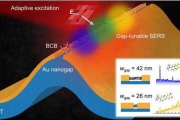
Real-time detection of infectious disease viruses
… by searching for molecular fingerprinting. A research team consisting of Professor Kyoung-Duck Park and Taeyoung Moon and Huitae Joo, PhD candidates, from the Department of Physics at Pohang University…

