New hybrid microscope probes nano-electronics
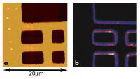
A false color SPIM image (b) reveals the same physical structure of a gold pattern on glass as an atomic force microscope image (a), but the high intensity regions in the SPIM image indicate that electron ejection is much more efficient at metal edge discontinuities. Credit: Credit: O.L.A. Monti, T.A. Baker, and D.J. Nesbitt/JILA
Scanning photoionization microscopy (SPIM), described in a new paper,* combines the high spatial resolution of optical microscopy with the high sensitivity to subtle electrical activity made possible by detecting the low-energy electrons emitted by a material as it is illuminated with laser pulses. The technique potentially could be used to make pictures of both electronic and physical patterns in devices such as nanostructured transistors or electrode sensors, or to identify chemicals or even elements in such structures.
“You make images by virtue of how readily electrons are photoejected from a material,” says NIST Fellow David Nesbitt, leader of the research group. “The method is in its infancy, but nevertheless it really does have the power to provide a new set of eyes for looking at nanostructured metals and semiconductors.”
The JILA-built apparatus includes a moving optical microscopy stage in a vacuum, an ultrafast near-ultraviolet laser beam that provides sufficient peak power to inject two photons (particles of light) into a metal at virtually the same time, and equipment for measuring the numbers and energy of electrons ejected from the material. By comparing SPIM images of nanostructured gold films to scans using atomic force microscopy, which profiles surface topology, the researchers confirmed the correlations and physical mapping accuracy of the new technique. They also determined that lines in SPIM images correspond to spikes in electron energy, or current, and that contrast depends on the depth of electrons escaping from the metal as well as variations in material thickness.
Work is continuing to further develop the method, which may be able to make chemically specific images, for example, if the lasers are tuned to different colors to affect only one type of molecule at a time.
Media Contact
More Information:
http://www.nist.govAll latest news from the category: Physics and Astronomy
This area deals with the fundamental laws and building blocks of nature and how they interact, the properties and the behavior of matter, and research into space and time and their structures.
innovations-report provides in-depth reports and articles on subjects such as astrophysics, laser technologies, nuclear, quantum, particle and solid-state physics, nanotechnologies, planetary research and findings (Mars, Venus) and developments related to the Hubble Telescope.


Newest articles

Zap Energy achieves 37-million-degree temperatures in a compact device
New publication reports record electron temperatures for a small-scale, sheared-flow-stabilized Z-pinch fusion device. In the nine decades since humans first produced fusion reactions, only a few fusion technologies have demonstrated…
Innovative microscopy demystifies metabolism of Alzheimer’s
Researchers at UC San Diego have deployed state-of-the art imaging techniques to discover the metabolism driving Alzheimer’s disease; results suggest new treatment strategies. Alzheimer’s disease causes significant problems with memory,…
A cause of immunodeficiency identified
After stroke and heart attack: Every year, between 250,000 and 300,000 people in Germany suffer from a stroke or heart attack. These patients suffer immune disturbances and are very frequently…

