Customized Y-shaped carbon nanotubes can compute
Researchers at UCSD and Clemson University have discovered that specially synthesized carbon nanotube structures exhibit electronic properties that are improved over conventional transistors used in computers. In a paper published* in the September issue of Nature Materials and released online on August 14, UCSD Mechanical and Aerospace Engineering professors Prabhakar Bandaru and Sungho Jin, graduate student Chiara Daraio, and Clemson physicist Apparao M. Rao reported that Y-shaped nanotubes behave as electronic switches similar to conventional MOS (metal oxide semiconductor) transistors, the workhorses of modern microprocessors, digital memory, and application-specific integrated circuits.
“This is the first time that a transistor-like structure has been fabricated using a branched carbon nanotube,” said Bandaru. “This discovery represents a new way of thinking about nano-electronic devices, and I think people interested in creating functionality at the nanoscale will be inspired to explore the ramifications of these Y-junction elements in greater detail.”
The stunning increase in the speed and power efficiency of electronics over the past two decades was primarily due to the steady shrinkage in size of conventional transistors. Chip makers have reduced the minimum feature size of transistors to about 100 nanometers, and that dimension is expected to shrink by the end of this decade. However, industry experts predict that fundamental technological and financial limits will prevent the makers of conventional MOS transistors to reduce their size much further. The Y-shaped nanotubes discussed in the Nature Materials paper are only a few tens of nanometers thick and can be made as thin as a few nanometers.
“The small size and dramatic switching behavior of these nanotubes makes them candidates for a new class of transistor,” said Bandaru.
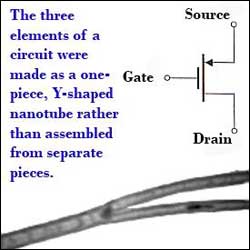
The new transistors were initially grown as straight nanotube elements. Titanium-modified iron catalyst particles added to the synthesis mixture were then attached to the straight nanotubes, nucleating additional growth, which continued like branches growing from a tree trunk. Consequently, the nascent nanotubes assumed a Y-shape with the catalyst particle gradually becoming absorbed at the junction of the stem and two branches.
When electrical contacts are attached to the nanotube structures, electrons travel into one arm of the Y, hop onto the catalyst particle, and then hop to the other arm and flow outward. Experiments conducted in Bandaru’s lab at UCSD’s Jacobs School of Engineering showed that the movement of electrons through the Y-junction can be finely controlled, or gated, by applying a voltage to the stem. Bandaru hypothesized that positive charge applied to the stem enhances the flow of electrons through the two arms, producing a strong “on” signal. Then, when the polarity of the charge is reversed, the movement of electrons through the arms essentially stops, creating an “off” signal. Such binary logic is the basis of nearly all transistors.
“Among electrical device engineers, this phenomenon is called gating,” said Bandaru. He said the phenomenon effectively makes Y-shaped nanotubes the smallest ready-made transistor yet, with rapid switching speeds and possible three-way gating capability. In earlier attempts to make carbon nanotube-based transistors, separate gates were added rather than built in.
“We think this discovery extends the paradigm of nanotechnology beyond just making things small,” said Bandaru. “We can synthesize functionality at the nanoscale, in this case to include the three elements of a circuit – the gate, source, and drain – and we don’t have to go to the trouble of making them separately and assembling them.”
The researchers plan to experiment with various other catalyst particles in order to tailor the three-way gating properties of the Y-junctions. “If we can easily fabricate, manipulate, and assemble these nano-devices on a large scale they could become the basis of a new kind of transistor and nanotechnology,” said Bandaru.
* “Novel electrical switching behaviour and logic in carbon nanotube Y-junctions,” P.R. Bandaru, C. Daraio, S. Jin and A.M. Rao, Nature Materials, September 2005
Media Contact
More Information:
http://www.ucsd.eduAll latest news from the category: Physics and Astronomy
This area deals with the fundamental laws and building blocks of nature and how they interact, the properties and the behavior of matter, and research into space and time and their structures.
innovations-report provides in-depth reports and articles on subjects such as astrophysics, laser technologies, nuclear, quantum, particle and solid-state physics, nanotechnologies, planetary research and findings (Mars, Venus) and developments related to the Hubble Telescope.


Newest articles

Superradiant atoms could push the boundaries of how precisely time can be measured
Superradiant atoms can help us measure time more precisely than ever. In a new study, researchers from the University of Copenhagen present a new method for measuring the time interval,…

Ion thermoelectric conversion devices for near room temperature
The electrode sheet of the thermoelectric device consists of ionic hydrogel, which is sandwiched between the electrodes to form, and the Prussian blue on the electrode undergoes a redox reaction…

Zap Energy achieves 37-million-degree temperatures in a compact device
New publication reports record electron temperatures for a small-scale, sheared-flow-stabilized Z-pinch fusion device. In the nine decades since humans first produced fusion reactions, only a few fusion technologies have demonstrated…

