Nanobridges Show Way to Nano Mass Production
They look like an elegant row of columns, tiny enough for atomic-scale hide-and-seek, but these colonnades represent a new way to bring nanotechnology into mass production.
Nanotechnology, the ability to create and work with structures and materials on an atomic scale, holds the promise of extreme miniaturization for electronics, chemical sensors and medical devices. But while researchers have created tiny silicon wires and connected them together one at a time, these methods cannot easily be scaled up.
“It takes weeks to make one or two, and you end up with different sizes and characteristics,” said M. Saif Islam, assistant professor of electrical and computer engineering, who joined UC Davis from Hewlett-Packard Laboratories in 2004.
Like handmade shoes, every manually assembled nanostructure comes out slightly different. Engineers would rather build devices the way cars or computers are built, with every item as consistent as possible.
While working at the Quantum Science Research group of Hewlett-Packard Laboratories, Islam and colleagues came up with a new approach. Silicon wafers used for building microcircuits are usually polished at one specific angle to the atomic planes of silicon. Instead, the group used a wafer that was polished at a different angle, changing the orientation of silicon atomic planes to the surface. Using a chemical vapor deposition technique, they could then grow identical, perpendicular columns of silicon.
The researchers have used this method to grow “nanobridges” across a gap between two vertical silicon electrodes. The nanobridges are strong, chemically stable and show better electrical properties than previous approaches, Islam said. They could be used for nanosized transistors, chemical sensors or lasers.
Taking the approach a step further, Islam and his colleagues at Hewlett-Packard made sandwiches of silicon and insulator and partly etched away the top layer to create awning-shaped structures of silicon supported by insulator. Silicon columns grown under the awnings form miniature colonnades.
The method allows engineers to combine nanowires of precise length with other silicon structures such as integrated circuits, he said.
At UC Davis, Islam plans to continue work on converting the technology into practical devices. The “nanobridge” technique was reported most recently in the March 2005 issue of the journal Applied Physics Part A. The nanocolonnade work was presented April 1 at the spring meeting of the Materials Research Society in San Francisco.
Media Contact
More Information:
http://www.ucdavis.eduAll latest news from the category: Physics and Astronomy
This area deals with the fundamental laws and building blocks of nature and how they interact, the properties and the behavior of matter, and research into space and time and their structures.
innovations-report provides in-depth reports and articles on subjects such as astrophysics, laser technologies, nuclear, quantum, particle and solid-state physics, nanotechnologies, planetary research and findings (Mars, Venus) and developments related to the Hubble Telescope.


Newest articles
Bringing bio-inspired robots to life
Nebraska researcher Eric Markvicka gets NSF CAREER Award to pursue manufacture of novel materials for soft robotics and stretchable electronics. Engineers are increasingly eager to develop robots that mimic the…

Bella moths use poison to attract mates
Scientists are closer to finding out how. Pyrrolizidine alkaloids are as bitter and toxic as they are hard to pronounce. They’re produced by several different types of plants and are…
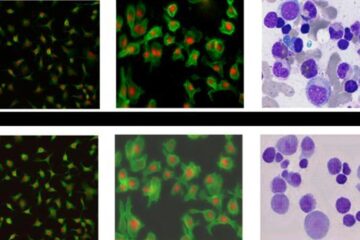
AI tool creates ‘synthetic’ images of cells
…for enhanced microscopy analysis. Observing individual cells through microscopes can reveal a range of important cell biological phenomena that frequently play a role in human diseases, but the process of…

