Breakthrough in advanced photonics manufacturing
The need for advanced highly integrated photonic circuits stems from the capacity expansion of telecommunications infrastructures driven by ever-increasing customer demand. Novel design and manufacturing technologies for advanced photonic circuits emerging from PICCO could meet this need.
Ready for mass production
The work of the IST programme-funded project has provided evidence that functional photonic circuits can be created using state-of-the-art deep UV lithography. This technology is at the very forefront of wafer-scale processing, and appears to be a promising approach for high-volume device production. The development has moved photonic crystals from a previous position as scientific curiosities to being serious contenders in the future manufacture of micro-photonic circuitry.
“We’ve established a design process for deep UV lithography that enables us to produce photonic crystals on an eight inch CMOS [complementary metal-oxide semiconductor] line,” says project coordinator Thomas Krauss of St Andrews University. “To date all photonics manufacturing has been done using e-beam lithography – we can now produce photonic circuits using deep UV lithography on an eight inch wafer – just like a vinyl disk – in one shot!”
Another objective was to demonstrate low-loss light propagation within waveguides defined by photonic microstructures, using conventional components but up to two orders of magnitude smaller. In principle the less amount of light lost (through scattering, etc.), the easier it is to produce complex circuits.
By calculating this light loss on a ’loss per device’ scale, project researchers were able to improve on conventional technology. Although the loss per centimetre figures were higher, with much smaller devices the total number of centimetres per device is less, so overall the light lost is reduced.
New CAD tool developed
Project participants also wanted to refine existing CAD tools and to develop a method of evaluating alternative circuit designs more easily. The result of this effort was an application called the ’CrystalWave’ design tool. CrystalWave is capable of designing and analysing photonic circuit designs in less that half of the time it would have taken previously, and can convert the results into production solutions that are ready for manufacturing.
The product comprises a layout editor, a Finite Difference Time Domain (FDTD) simulation application that is 2.5 times faster and requires a quarter of the memory of comparable commercial 3D software, and GDS II software to convert the modelled structure directly into a file for lithographic pattern generation. Significantly, all of these applications run on desktop PCs.
Widening market opportunities
According to Krauss, the results of PICCO are a significant contributor to maintaining European research at the forefront of this field, as micro-photonics will play a key role in the telecoms backbone in the longer term. Japanese research in the field predicts that circuits with 10,000 components will be deployed inside the next 10 years; photonic circuitry is the only means of achieving this goal.
PICCO’s success in developing deep UV lithography methods for wafer-scale fabrication of photonic circuits significantly widens the market opportunities for this technology. Bringing deep UV lithography to a mass-production basis lays the foundations for low-cost high-functionality micro-optic components. Such advances can give the optical component companies a substantial competitive advantage.
All of the academic partners involved in the project have been awarded additional funding in order to further develop the photonics research base. In addition a number of patents have been taken out by some of the PICCO partners, further strengthening their position in the photonics market.
PICCO has also directly contributed to the success and growth of the SME Photon Design Ltd. Oxford, UK, which, through its involvement in the project, has been able to gain a foothold for its products in the promising market of CAD tools for high contrast microstructures. The company is now marketing its CrystalWave design tool commercially, taking the company into two new market areas – mask production and the FDTD simulation technique. Equally, the success of PICCO has influenced Pirelli in developing their microphotonics capability via the establishment of a brand new microfabrication laboratory in Milan, Italy.
“There are two main reasons for the success and the world-wide recognition of PICCO,” says EC scientific officer Henri Rajbenbach. “The first is that the PICCO partners had a very early understanding that photonics has to exploit synergies with the more traditional micro-electronics technologies such as deep UV lithography. In itself, this is insufficient; the second reason for success is the outstanding contribution of individual young researchers in convincing this silicon community to open one production line to photonics-aficionados for the ultimate realisation of novel devices.” “It is my hope that this can develop into a platform to serve the photonic community at large, and contribute to the building of an Optics and Photonics European Research Area. But work still remains. At this stage, these PICCO devices are passive; future work will tell us if this research avenue is also viable for active, light-emitting components,” Rajbenbach concludes.
Contact:
Prof Thomas Krauss
Saint Andrews University
School for Physics and Astronomy
North Haugh
St Andrews KY16 9SS
United Kingdom
Tel: +44-1334-463107
Email: tfk@st-andrews.ac.uk
Source: Based on information from PICCO
Media Contact
All latest news from the category: Physics and Astronomy
This area deals with the fundamental laws and building blocks of nature and how they interact, the properties and the behavior of matter, and research into space and time and their structures.
innovations-report provides in-depth reports and articles on subjects such as astrophysics, laser technologies, nuclear, quantum, particle and solid-state physics, nanotechnologies, planetary research and findings (Mars, Venus) and developments related to the Hubble Telescope.


Newest articles
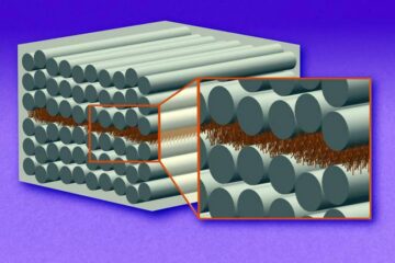
“Nanostitches” enable lighter and tougher composite materials
In research that may lead to next-generation airplanes and spacecraft, MIT engineers used carbon nanotubes to prevent cracking in multilayered composites. To save on fuel and reduce aircraft emissions, engineers…
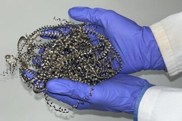
Trash to treasure
Researchers turn metal waste into catalyst for hydrogen. Scientists have found a way to transform metal waste into a highly efficient catalyst to make hydrogen from water, a discovery that…
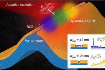
Real-time detection of infectious disease viruses
… by searching for molecular fingerprinting. A research team consisting of Professor Kyoung-Duck Park and Taeyoung Moon and Huitae Joo, PhD candidates, from the Department of Physics at Pohang University…

