Copper nanowires grown by new process create long-lasting displays

“We can grow forests of freestanding copper nanowires of controlled diameter and length, suitable for integration into electronic devices,” said Kyekyoon (Kevin) Kim, a professor of electrical and computer engineering.
“The copper nanowires are grown on a variety of surfaces, including glass, metal and plastic by chemical vapor deposition from a precursor,” said Hyungsoo Choi, a research professor in the Micro and Nanotechnology Laboratory and in the department of electrical and computer engineering. “The patented growth process is compatible with contemporary silicon-processing protocols.”
The researchers describe the nanowires, the growth process, and a proof-of-principle field-emission display in a paper accepted for publication in the journal Advanced Materials, and posted on its Web site.
Typically, the nanowires of 70 to 250 nanometers in diameter are grown on a silicon substrate at temperatures of 200 to 300 degrees Celsius and require no seed or catalyst. The size of the nanowires is controlled by the processing conditions, such as substrate, substrate temperature, deposition time and precursor feeding rate. The columnar, five-sided nanowires terminate in sharp, pentagonal tips that facilitate electron emission.
To demonstrate the practicability of the low-temperature growth process, the researchers first grew an array of copper nanowires on a patterned silicon substrate. Then they fashioned a field-emission display based on the array’s bundles of nanowires.
In a field-emission display, electrons emitted from the nanowire tips strike a phosphor coating to produce an image. Because the researchers used a bundle of nanowires for each pixel in their display, the failure of a few nanowires will not ruin the device.
“The emission characteristics of the copper nanowires in our proof-of-principle field-emission display were very good,” said Kim, who also is affiliated with the U. of I.’s department of materials science and engineering, department of bioengineering, department of nuclear, plasma and radiological engineering, Beckman Institute, Micro and Nanotechnology Laboratory, and the Institute for Genomic Biology. “Our experimental results suggest bundled nanowires could lead to longer lasting field-emission displays.”
In addition to working on flexible displays made from copper nanowires grown on bendable plastic, the researchers are also working on silver nanowires.
With Kim and Choi, co-authors of the paper are graduate student and lead author Chang Wook Kim, graduate student Wenhua Gu, postdoctoral research associate Martha Briceno, and professor and head of materials science and engineering Ian Robertson.
Funding was provided by the University of Illinois. Characterization of the samples was conducted at the university’s Center for Microanalysis of Materials, which is partially funded by the U.S. Department of Energy.
To reach Kyekyoon Kim, call 217-333-7162; e-mail: kevinkim@uiuc.edu.
To reach Hyungsoo Choi, call 217-244-6345; e-mail: hyungsoo@uiuc.edu.
Media Contact
All latest news from the category: Physics and Astronomy
This area deals with the fundamental laws and building blocks of nature and how they interact, the properties and the behavior of matter, and research into space and time and their structures.
innovations-report provides in-depth reports and articles on subjects such as astrophysics, laser technologies, nuclear, quantum, particle and solid-state physics, nanotechnologies, planetary research and findings (Mars, Venus) and developments related to the Hubble Telescope.
Newest articles
Superradiant atoms could push the boundaries of how precisely time can be measured
Superradiant atoms can help us measure time more precisely than ever. In a new study, researchers from the University of Copenhagen present a new method for measuring the time interval,…
Ion thermoelectric conversion devices for near room temperature
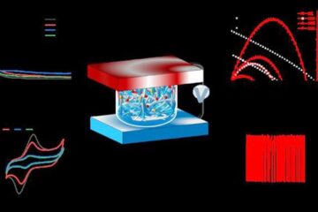
The electrode sheet of the thermoelectric device consists of ionic hydrogel, which is sandwiched between the electrodes to form, and the Prussian blue on the electrode undergoes a redox reaction…
Zap Energy achieves 37-million-degree temperatures in a compact device
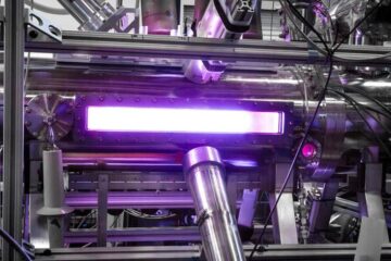
New publication reports record electron temperatures for a small-scale, sheared-flow-stabilized Z-pinch fusion device. In the nine decades since humans first produced fusion reactions, only a few fusion technologies have demonstrated…


