Nanodevices: Theory goes big
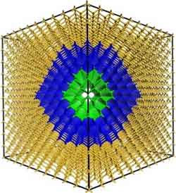
The structure of a small-diameter (green) and large-diameter (blue) silicon nanowire, inside a bulk silicon (yellow) structure<br>Copyright : A*STAR
Silicon nanowires are widely recognized as candidates for use in next-generation sensors, battery electrodes and solar cells, and first-principle calculations are an important tool in the development of these applications. Most of the calculations performed so far have only considered nanowires with diameters of less than 4 nanometers, although in practice, nanowire devices typically have much larger diameters.
Man-Fai Ng at the A*STAR Institute of High Performance Computing and co-workers in Singapore1 have now performed first-principle calculations to simulate the properties of silicon nanowires with diameters of up to 7.3 nanometers (see image). The researchers have examined nanowires ranging from atomic scales (~1 nanometer diameters) to the large-diameter limit, at which point they begin to resemble bulk silicon. The researchers studied the nanowire bandgap — a key parameter that affects both electrical and optical properties — and found that this decreased with increasing diameter. The simulation results were consistent with those obtained from experiment, and the trend was more predictable at larger diameters.
Ng and his co-workers also studied how the ‘direct’ and ‘indirect’ bandgaps change when the diameter of the silicon nanowire increases. Bulk silicon has an indirect bandgap, which means that the excitation of a mobile charge carrier must be accompanied by a simultaneous change in its momentum. Because this is relatively unlikely, bulk silicon is a poor absorber and emitter of light. Semiconductors with direct bandgaps, on the other hand, are optically active. The team of reseachers found that silicon nanowire bandgaps assumed indirect characteristics above diameters of around 4 nanometers, and direct characteristics for smaller diameters.
The researchers were also able to calculate the way in which nanowire diameter affects the location of dopant atoms along the nanowire radius. “Foreign atoms like boron are used to increase the density of mobile charges, and their exact location can have a strong effect on nanowire behavior,” says Ng. “We showed that boron-dopant atoms are more likely to be found at both the nanowire core and surface in larger-diameter nanowires, and mainly at the surface for smaller diameters.”
Ng and his co-workers envision that elucidating the relationship between bandgap and diameter will be useful for the development of nanoscale silicon devices. The work is also significant as a proof of principle. “As computational resources continue to improve and drop in price, the demand for first-principles simulations of large-scale problems will grow. Our work demonstrates the feasibility of addressing one such problem,” says Ng.
The A*STAR-affiliated researchers contributing to this research are from the Institute of High Performance Computing
Media Contact
All latest news from the category: Physics and Astronomy
This area deals with the fundamental laws and building blocks of nature and how they interact, the properties and the behavior of matter, and research into space and time and their structures.
innovations-report provides in-depth reports and articles on subjects such as astrophysics, laser technologies, nuclear, quantum, particle and solid-state physics, nanotechnologies, planetary research and findings (Mars, Venus) and developments related to the Hubble Telescope.


Newest articles
Stretchable quantum dot display
Intrinsically stretchable quantum dot-based light-emitting diodes achieved record-breaking performance. A team of South Korean scientists led by Professor KIM Dae-Hyeong of the Center for Nanoparticle Research within the Institute for…
Internet can achieve quantum speed with light saved as sound
Researchers at the University of Copenhagen’s Niels Bohr Institute have developed a new way to create quantum memory: A small drum can store data sent with light in its sonic…

A chip unique in the world
A team from UPV and iPRONICS has manufactured the first universal, programmable and multifunctional photonic chip on the market. A team from the Photonics Research Laboratory (PRL)-iTEAM of the Universitat…

