Making a layer cake with atomic precision

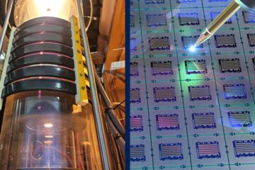
The team used individual one-atom-thick crystals to construct a multilayer cake that works as a nanoscale electric transformer.
Graphene, isolated for the first time at The University of Manchester in 2004, has the potential to revolutionise diverse applications from smartphones and ultrafast broadband to drug delivery and computer chips.
It has the potential to replace existing materials, such as silicon, but the Manchester researchers believe it could truly find its place with new devices and materials yet to be invented.
In the nanoscale transformer, electrons moving in one metallic layer pull electrons in the second metallic layer by using their local electric fields. To operate on this principle, the metallic layers need to be insulated electrically from each other but separated by no more than a few interatomic distances, a giant leap from the existing nanotechnologies.
These new structures could pave the way for a new range of complex and detailed electronic and photonic devices which no other existing material could make, which include various novel architectures for transistors and detectors.
The scientists used graphene as a one-atom-thick conductive plane while just four atomic layers of boron nitride served as an electrical insulator.
The researchers started with extracting individual atomic planes from bulk graphite and boron nitride by using the same technique that led to the Nobel Prize for graphene, a single atomic layer of carbon. Then, they used advanced nanotechnology to mechanically assemble the crystallites one by one, in a Lego style, into a crystal with the desired sequence of planes.
The nano-transformer was assembled by Dr Roman Gorbachev, of The University of Manchester, who described the required skills. He said: “Every Russian and many in the West know The Tale of the Clockwork Steel Flea.
“It could only be seen through the most powerful microscope but still danced and even had tiny horseshoes. Our atomic-scale Lego perhaps is the next step of craftsmanship”.
Professor Geim added: “The work proves that complex devices with various functionalities can be constructed plane by plane with atomic precision.
“There is a whole library of atomically-thin materials. By combining them, it is possible to create principally new materials that don't exist in nature. This avenue promises to become even more exciting than graphene itself.”
Media Contact
More Information:
http://www.manchester.ac.ukAll latest news from the category: Physics and Astronomy
This area deals with the fundamental laws and building blocks of nature and how they interact, the properties and the behavior of matter, and research into space and time and their structures.
innovations-report provides in-depth reports and articles on subjects such as astrophysics, laser technologies, nuclear, quantum, particle and solid-state physics, nanotechnologies, planetary research and findings (Mars, Venus) and developments related to the Hubble Telescope.
Newest articles

Silicon Carbide Innovation Alliance to drive industrial-scale semiconductor work
Known for its ability to withstand extreme environments and high voltages, silicon carbide (SiC) is a semiconducting material made up of silicon and carbon atoms arranged into crystals that is…

New SPECT/CT technique shows impressive biomarker identification
…offers increased access for prostate cancer patients. A novel SPECT/CT acquisition method can accurately detect radiopharmaceutical biodistribution in a convenient manner for prostate cancer patients, opening the door for more…

How 3D printers can give robots a soft touch
Soft skin coverings and touch sensors have emerged as a promising feature for robots that are both safer and more intuitive for human interaction, but they are expensive and difficult…


