Laser physics: Getting silicon into order
Copyright : iStockphoto.com/ason <br>
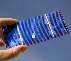
The importance of silicon for almost every element in modern-day electronic devices and computers is due largely to its crystalline atomic structure. Crystalline silicon, however, is much more expensive to produce than its non-crystalline or amorphous form, which has limited the cost reduction achievable in devices such as silicon-based solar cells.
Xincai Wang at the A*STAR Singapore Institute of Manufacturing Technology and co-workers[1] have now shown that ultrafast pulses of light can be used to crystallize amorphous silicon and to texture its surface.
The useful electronic properties of silicon stem from the way the atoms are arranged into a regular and repeating lattice. Amorphous silicon, on the other hand, does not display this long-range order: nearby atoms are bonded in the same way but the structure is not homogenous through the whole material. While lacking the extraordinarily useful properties of its crystalline relative, amorphous silicon does have some advantages. Thin films of amorphous silicon can be grown at low temperatures and therefore at much lower cost. In fact, amorphous silicon is used widely in the field of photovoltaics for the conversion of sunlight into electrical power. But modifying the material could improve both electrical efficiency and optical sensitivity.
The researchers used laser radiation to achieve this level of material control. They focused pulses of light just 150 femtoseconds in duration into a spot 30 micrometers in diameter. This spot was then scanned across an 80-nanometer-thick layer of amorphous silicon deposited on a glass substrate.
The first noticeable effect was a change in color: the treated area was darker than the untreated region. Closer inspection using an electron microscope revealed that the laser created ‘nano-spikes’ in the silicon. This texturing is useful for photovoltaic applications because it reduces light reflection from the surface and thereby increases absorption: an effect the researchers confirmed directly.
Raman spectroscopy—a powerful technique for analyzing atomic structure—was then used to compare treated and untreated samples. The Raman spectrum for the untreated region had two peaks characteristic of an amorphous structure. But that of the treated sample displayed a third sharper peak indicative of a crystalline atomic structure. This state change was likely caused by the excitation of electrons at the surface of the silicon by the laser pulses, which weakened the interatomic bonds in a way fundamentally different from simple thermal melting.
“Our process has potential applications in the fabrication of high-efficiency thin-film silicon for solar cells, as well as thin-film transistors and other novel optoelectronic devices,” says Wang.
The A*STAR-affiliated researchers contributing to this research are from the Singapore Institute of Manufacturing Technology
Journal information
[1] Wang, X.C. et al. Femtosecond laser induced surface nanostructuring and simultaneous crystallization of amorphous thin silicon film. Optics Express 18, 19379–19385 (2010).
Media Contact
All latest news from the category: Physics and Astronomy
This area deals with the fundamental laws and building blocks of nature and how they interact, the properties and the behavior of matter, and research into space and time and their structures.
innovations-report provides in-depth reports and articles on subjects such as astrophysics, laser technologies, nuclear, quantum, particle and solid-state physics, nanotechnologies, planetary research and findings (Mars, Venus) and developments related to the Hubble Telescope.


Newest articles
“Nanostitches” enable lighter and tougher composite materials
In research that may lead to next-generation airplanes and spacecraft, MIT engineers used carbon nanotubes to prevent cracking in multilayered composites. To save on fuel and reduce aircraft emissions, engineers…
Trash to treasure
Researchers turn metal waste into catalyst for hydrogen. Scientists have found a way to transform metal waste into a highly efficient catalyst to make hydrogen from water, a discovery that…
Real-time detection of infectious disease viruses
… by searching for molecular fingerprinting. A research team consisting of Professor Kyoung-Duck Park and Taeyoung Moon and Huitae Joo, PhD candidates, from the Department of Physics at Pohang University…

