Individual quantum dots imaged in 3-D for first time
This is a conventional STM image of a quantum dot, top, compared with an image produced using the new excited-state SMA-STM technique. Credit: Martin Gruebele Usage Restrictions: Graphic may be used with stories related to this press release. Credit is required. Graphic courtesy Martin Gruebele.
The findings, published in The Journal of Chemical Physics, brought together researchers from the University of Illinois and the University of Washington, Seattle in a collaborative project through the Beckman Institute for Advanced Science and Technology at the U. of I.
Nanostructures like microchip semiconductors, carbon nanotubes and large protein molecules contain defects that form during synthesis that cause them to differ in composition from one another. However, these defects are not always a bad thing, said Martin Gruebele, the lead author and an Illinois chemistry professor and chair.
“The term 'defect' is a bit of a misnomer,” Gruebele said. “For example, semiconductors are manufactured with intentional defects that form the 'holes' that electrons jump into to produce electrical conductivity. Having the ability to image those defects could let us better characterize them and control their production.”
As advances in technology allow for smaller and smaller nanoparticles, it is critical for engineers to know the precise number and location of these defects to assure quality and functionality.
The study focused on a class of nanoparticles called quantum dots. These dots are tiny, near-spherical semiconductors used in technology like solar panels, live cell imaging and molecular electronics – the basis for quantum computing.
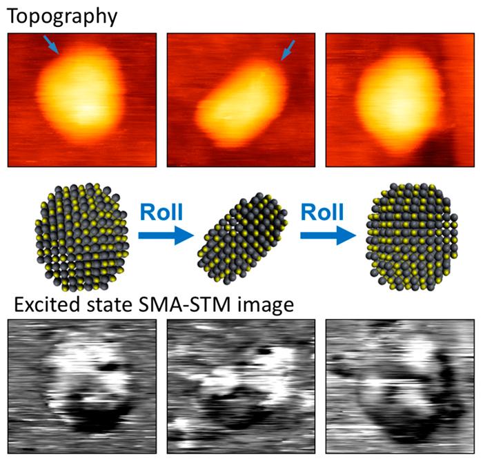
The team observed the quantum dots using a single-molecule absorption scanning tunneling microscope fitted with a needle sharpened to a thickness of only one atom at its tip. The needle nudges the individual particles around on a surface and scans them to get a view of the quantum dot from different orientations to produce a 3-D image.
The researchers said there are two distinct advantages of the new SMA-STM method when compared with the current technology – the Nobel Prize-winning technique called cryogenic electron tomography.
For a video related to this research can be found here.
“Instead of an image produced using an average of thousands of different particles, as is done with CryoET, SMA-STM can produce an image from a single particle in about 20 different orientations,” Gruebele said. “And because we are not required to chill the particles to near-absolute zero temperatures, we can capture the particles at room temperature, not frozen and motionless.”
The researchers looked at semiconductor quantum dots for this study, but SMA-STM can also be used to explore other nanostructures such as carbon nanotubes, metal nanoparticles or synthetic macromolecules. The group believes the technique can be refined for use with soft materials like protein molecules, Gruebele said.
The researchers are working to advance SMA-STM into a single-particle tomography technique, meaning that they will need to prove that method is noninvasive.
“For SMA-STM to become a true single-particle tomography technique, we will need to prove that our nudges do not damage or score the nanoparticle in any way while rolled around,” Gruebele said. “Knocking off just one atom can fundamentally alter the defect structure of the nanoparticle.”
###
The National Science Foundation, the Eiszner Family Foundation and the Beckman Institute supported this research.
Editor's notes:
To reach Martin Gruebele, call 217-333-1624; mgruebel@illinois.edu.
The paper “Orientation-dependent imaging of electronically excited quantum dots” is available online and from the U. of I. News Bureau.
DOI: 10.1063/1.5012784
Media Contact
All latest news from the category: Physics and Astronomy
This area deals with the fundamental laws and building blocks of nature and how they interact, the properties and the behavior of matter, and research into space and time and their structures.
innovations-report provides in-depth reports and articles on subjects such as astrophysics, laser technologies, nuclear, quantum, particle and solid-state physics, nanotechnologies, planetary research and findings (Mars, Venus) and developments related to the Hubble Telescope.


Newest articles

Properties of new materials for microchips
… can now be measured well. Reseachers of Delft University of Technology demonstrated measuring performance properties of ultrathin silicon membranes. Making ever smaller and more powerful chips requires new ultrathin…

Floating solar’s potential
… to support sustainable development by addressing climate, water, and energy goals holistically. A new study published this week in Nature Energy raises the potential for floating solar photovoltaics (FPV)…

Skyrmions move at record speeds
… a step towards the computing of the future. An international research team led by scientists from the CNRS1 has discovered that the magnetic nanobubbles2 known as skyrmions can be…

