Gentler processing may yield better molecular devices
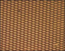
Copper contact deposition on organic electronic molecules using the NIST patented process is highly specific, an important feature for building dense arrays of devices. Shown here is a cross-hatched pattern of copper deposits on 10-micrometer-wide, single-layer strips of molecules that have been bound to a gold substrate with microcontact printing.
A simple, chemical way to attach electrical contacts to molecular-scale electronic components has been developed by researchers at the National Institute of Standards and Technology (NIST). The recently patented* method attaches a layer of copper on the ends of delicate molecular components to avoid damage to the components that commonly occurs with conventional techniques.
Molecular electronics–designing carbon-based molecules to act as wires, diodes, transistors and other microelectronic devices–is one of the most dynamic frontiers in nanotechnology. An area equal to the cross-section of a typical human hair might hold about a thousand semiconductor transistors at the current state of art, but up to 13 million molecular transistors.
A key challenge in molecular electronics is making electrical contacts to the fragile molecules, chemical chains that are easily damaged. Currently, this is most often done by vaporizing a metal onto the molecules that stand like blades of grass on a metal substrate. The vaporized metal atoms are supposed to settle on the tops of the molecules but they also often eat away at the delicate structures, or fall through gaps in the “turf” and short out the device. Yields of working devices are typically only a few percent.
NIST researchers designed a technique in which the molecules are synthesized with an additional chemical group attached to the top of the molecule. The chip is immersed in a solution including copper ions, which preferentially bind to the added group, forming a strong, chemically bonded contact that also protects the underlying molecule during further metallic vapor deposition steps. Tests at NIST have demonstrated that the technique works well on surfaces patterned with microcontact printing, producing clean, sharply defined edges, important for the fabrication of practical devices.
Media Contact
All latest news from the category: Life Sciences and Chemistry
Articles and reports from the Life Sciences and chemistry area deal with applied and basic research into modern biology, chemistry and human medicine.
Valuable information can be found on a range of life sciences fields including bacteriology, biochemistry, bionics, bioinformatics, biophysics, biotechnology, genetics, geobotany, human biology, marine biology, microbiology, molecular biology, cellular biology, zoology, bioinorganic chemistry, microchemistry and environmental chemistry.


Newest articles

Properties of new materials for microchips
… can now be measured well. Reseachers of Delft University of Technology demonstrated measuring performance properties of ultrathin silicon membranes. Making ever smaller and more powerful chips requires new ultrathin…

Floating solar’s potential
… to support sustainable development by addressing climate, water, and energy goals holistically. A new study published this week in Nature Energy raises the potential for floating solar photovoltaics (FPV)…

Skyrmions move at record speeds
… a step towards the computing of the future. An international research team led by scientists from the CNRS1 has discovered that the magnetic nanobubbles2 known as skyrmions can be…

