Energy-saving minicomputers for the ‘Internet of Things’
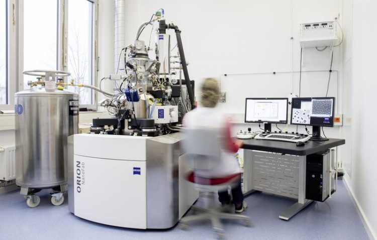
HZDR’s ion microscope produces a highly focused neon beam that allows for the local mixing of atoms in thin layered stacks. Tempering these stacks, silicon single quantum dots form on their own. HZDR / Oliver Killig
“Billions of tiny computers will in future communicate with each other via the Internet or locally. Yet power consumption currently remains a great obstacle”, says project coordinator Dr. Johannes von Borany from the HZDR. “Basically, there are two options: either one improves the batteries or one develops computer chips that require significantly less energy.”
For example, it has been known for years that single electron transistors are an energy-saving alternative to the commonly used field effect transistors (FET). As yet, however, they only work at low temperatures and, what is more, they are not compatible with the so-called CMOS technology that forms the technological basis for the integration of a huge number of FET components on a computer chip necessary to perform complex signal processing at laptops or smartphones.
The single electron transistor (SET) switches electricity by means of a single electron. The novel SET is based on a so-called quantum dot (consisting of just several hundred silicon atoms) embedded in an isolating layer that is sandwiched between two conducting layers.
In order for a SET to function at room temperature, the silicon quantum dot needs to be smaller than five nanometers (1 nanometer = 1 millionth of a millimeter). Yet the electrons would not be able to pass through the transistor without another requirement being fulfilled: the distance between the quantum dot and the conducting layers must not be larger than two to three nanometers. As yet, these requirements could not be realized in nanoelectronics.
Self-organization of silicon nanodots in nanopillars
“Our transistor is based on a nanopillar. We have discovered a mechanism that ensures that the silicon quantum dot virtually form on their own”, says Dr. Karl-Heinz Heinig, initiator of the new EU project. “We construct slim silicon pillars of about 20 nanometers into which we embed a six nanometer thin layer consisting of the isolator silicon dioxide.
Silicon atoms are pushed into the isolator by irradiating the nanopillar with fast, charged particles. When the structures are subsequently subjected to strong heat, the atoms cluster at the center of the isolating layer to form a single silicon quantum dot.” Leading European research institutions as well as the major players in the semiconductor industry, Globalfoundries, X-FAB and STMicroelectronics, have joined forces in the project to achieve the ability of reliably producing and reproducing billions of SET components made of nanopillars.
Demonstrator with two kinds of transistors: SET and FET complement each other
While CEA-Leti, a renowned French research institute for microelectronics, will produce the nanopillars with such a small size not yet achieved so far, the Spanish National Centre for Microelectronics in Barcelona (CSIC) is commissioned to build the demonstrator that will constitute the conclusion of the four-year EU project. However, the task the researchers have set themselves is actually far more complicated.
The demonstrator cannot consist only of SET components that carry out the logical operations at room temperature. Classical FET components are an additional requirement, also in the form of nanopillars. Why? The energy-saving single electron transistors have too little power available to interact with the world outside their own chip. This is why the chip that should facilitate the triumphant advance of the ‘Internet of Things’ will contain FET in addition to SET nanopillars so that the former will be able to transmit the results of the SET operations to other chips and devices.
Kick-off meeting for ‘Ions4Set’ from February 1 to 3 at the HZDR
The first meeting of all partners involved in this EU project will take place from February 1 to 3, 2016 at the Helmholtz-Zentrum Dresden-Rossendorf. Other partners in addition to the HZDR, CEA-Leti and CSIC are the Fraunhofer Institute for Integrated Systems and Device Technology IISB in Erlangen in Germany, the Institute for Microelectronics and Microsystems IMM at the CNR in Italy and the University of Helsinki in Finland. The project is scheduled to run for four years, the funding is four million euro.
Dr. Heinig from the HZDR is optimistic: “We are convinced of successfully completing the new project. On the one hand, we draw on insights from a previous EU project with computer chip producers; on the other, we were able to win over the leading research institutions in this field to be our partners.”
And last but not least, the strengths of the HZDR’s Ion Beam Center will make an impact regarding the central process steps for producing single electron transistors: many years of experience in materials research, a wide range of ion accelerators as well as state-of-the-art physical analysis procedures. “After the successful completion of the project, it will be straightforward for the microelectronics industry to adopt our manufacturing technique as fully compatible with CMOS technology”, Dr. Heinig emphasizes.
Further information:
Dr. Johannes von Borany / Dr. Karl-Heinz Heinig
Institute of Ion Beam Physics and Materials Research at HZDR
Phone +49 351 260-3378 / -3288
Mail: j.v.borany@hzdr.de / k.h.heinig@hzdr.de
Media contact:
Dr. Christine Bohnet | Press officer
Phone +49 351 260-2450 | Mail: c.bohnet@hzdr.de
Helmholtz-Zentrum Dresden-Rossendorf | Bautzner Landstr. 400 | 01328 Dresden |
The Helmholtz-Zentrum Dresden-Rossendorf (HZDR) conducts research in the sectors energy, health, and matter. It focuses its research on the following topics:
• How can energy and resources be used efficiently, safely, and sustainably?
• How can malignant tumors be visualized and characterized more precisely and treated effectively?
• How do matter and materials behave in strong fields and in the smallest dimensions?
The HZDR has been a member of the Helmholtz Association, Germany’s largest research organization, since 2011. It has four locations (Dresden, Leipzig, Freiberg, Grenoble) and employs about 1,100 people – approximately 500 of whom are scientists, including 150 doctoral candidates.
Media Contact
All latest news from the category: Information Technology
Here you can find a summary of innovations in the fields of information and data processing and up-to-date developments on IT equipment and hardware.
This area covers topics such as IT services, IT architectures, IT management and telecommunications.


Newest articles

Properties of new materials for microchips
… can now be measured well. Reseachers of Delft University of Technology demonstrated measuring performance properties of ultrathin silicon membranes. Making ever smaller and more powerful chips requires new ultrathin…

Floating solar’s potential
… to support sustainable development by addressing climate, water, and energy goals holistically. A new study published this week in Nature Energy raises the potential for floating solar photovoltaics (FPV)…

Skyrmions move at record speeds
… a step towards the computing of the future. An international research team led by scientists from the CNRS1 has discovered that the magnetic nanobubbles2 known as skyrmions can be…

