UCLA researchers demonstrate fully printed carbon nanotube transistor circuits for displays
OLED-based displays are now used in cell phones, digital cameras and other portable devices. But developing a lower-cost method for mass-producing such displays has been complicated by the difficulties of incorporating thin-film transistors that use amorphous silicon and polysilicon into the production process.
Now, researchers from Aneeve Nanotechnologies, a startup company at UCLA's on-campus technology incubator at the California NanoSystems Institute (CNSI), have used low-cost ink-jet printing to fabricate the first circuits composed of fully printed back-gated and top-gated carbon nanotube–based electronics for use with OLED displays. The research was published this month in the journal Nano Letters.
The startup includes collaborators from the departments of materials science and electrical engineering at the UCLA Henry Samueli School of Engineering and Applied Science and the department of electrical engineering at the University of Southern California.
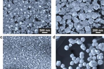
In this innovative study, the team made carbon nanotube thin-film transistors with high mobility and a high on–off ratio, completely based on ink-jet printing. They demonstrated the first fully printed single-pixel OLED control circuits, and their fully printed thin-film circuits showed significant performance advantages over traditional organic-based printed electronics.
“This is the first practical demonstration of carbon nanotube–based printed circuits for display backplane applications,” said Kos Galatsis, an associate adjunct professor of materials science at UCLA Engineering and a co-founder of Aneeve. “We have demonstrated carbon nanotubes' viable candidacy as a competing technology alongside amorphous silicon and metal-oxide semiconductor solution as a low-cost and scalable backplane option.”
This distinct process utilizes an ink-jet printing method that eliminates the need for expensive vacuum equipment and lends itself to scalable manufacturing and roll-to-roll printing. The team solved many material integration problems, developed new cleaning processes and created new methods for negotiating nano-based ink solutions.
For active-matrix OLED applications, the printed carbon nanotube transistors will be fully integrated with OLED arrays, the researchers said. The encapsulation technology developed for OLEDs will also keep the carbon nanotube transistors well protected, as the organics in OLEDs are very sensitive to oxygen and moisture.
The technology incubator at the CNSI was established two years ago to nurture early-stage research and to help speed the commercial translation of technologies developed at UCLA. Aneeve Nanotechnologies LLC has been conducting proof-of-concept work at the tech incubator with the mission of developing superior, low-cost, high-performance electronics using nanotechnology solutions that bridge the gap between emerging and traditional platforms.
The California NanoSystems Institute is an integrated research facility located at UCLA and UC Santa Barbara. Its mission is to foster interdisciplinary collaborations in nanoscience and nanotechnology; to train a new generation of scientists, educators and technology leaders; to generate partnerships with industry; and to contribute to the economic development and the social well-being of California, the United States and the world. The CNSI was established in 2000 with $100 million from the state of California. The total amount of research funding in nanoscience and nanotechnology awarded to CNSI members has risen to over $900 million. UCLA CNSI members are drawn from UCLA's College of Letters and Science, the David Geffen School of Medicine, the School of Dentistry, the School of Public Health and the Henry Samueli School of Engineering and Applied Science. They are engaged in measuring, modifying and manipulating atoms and molecules — the building blocks of our world. Their work is carried out in an integrated laboratory environment. This dynamic research setting has enhanced understanding of phenomena at the nanoscale and promises to produce important discoveries in health, energy, the environment and information technology.
For more news, visit the UCLA Newsroom and follow us on Twitter.
Media Contact
More Information:
http://www.ucla.eduAll latest news from the category: Power and Electrical Engineering
This topic covers issues related to energy generation, conversion, transportation and consumption and how the industry is addressing the challenge of energy efficiency in general.
innovations-report provides in-depth and informative reports and articles on subjects ranging from wind energy, fuel cell technology, solar energy, geothermal energy, petroleum, gas, nuclear engineering, alternative energy and energy efficiency to fusion, hydrogen and superconductor technologies.


Newest articles
Making diamonds at ambient pressure
Scientists develop novel liquid metal alloy system to synthesize diamond under moderate conditions. Did you know that 99% of synthetic diamonds are currently produced using high-pressure and high-temperature (HPHT) methods?[2]…

Eruption of mega-magnetic star lights up nearby galaxy
Thanks to ESA satellites, an international team including UNIGE researchers has detected a giant eruption coming from a magnetar, an extremely magnetic neutron star. While ESA’s satellite INTEGRAL was observing…

Solving the riddle of the sphingolipids in coronary artery disease
Weill Cornell Medicine investigators have uncovered a way to unleash in blood vessels the protective effects of a type of fat-related molecule known as a sphingolipid, suggesting a promising new…

