Semiconductor interfaces: Big opportunities for tiny insulators
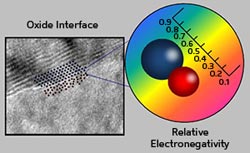
A new theoretical model enables accurate predictions of dipoles at oxide interfaces (left, electron microscopy image) using the classical property of electronegativity (right). The scale shows how two elements with different relative electronegativities align at an interface.<br><br><br><br>Copyright : © 2013 A*STAR Institute of Materials Research and Engineering<br>
Advances in miniaturization have made electronic devices cheaper and more powerful, but these procedures also create new challenges for materials scientists. For example, traditional silicon dioxide insulators used in field-effect transistors begin to leak small amounts of current at nanoscale dimensions.
To combat this problem, researchers have developed insulators called ‘high-k dielectrics’ that link heavier elements, such as hafnium or zirconium, into insulating oxide films with exceptional charge-isolating capabilities.
Integrating high-k dielectrics into circuits, however, creates a different manufacturing problem. Localized electric fields known as charged dipoles can form at insulator–semiconductor interfaces and generate unwanted voltages that impact device performance. Sing Yang Chiam from the A*STAR Institute of Materials Research and Engineering in Singapore and co-workers have now developed a model that can identify interface dipole problems before they appear1 — a finding that promises to help end the ‘trial-and-error’ design issues typical of high-k dielectrics.
Currently, materials scientists employ extensive quantum mechanical calculations to determine whether or not new high-k dielectrics will have interface dipoles. Chiam and co-workers investigated a more intuitive approach: they linked the appearance of interface dipoles to the classical property of electronegativity, a number that relates an element’s electron-attracting power to its position in the periodic table.
Scientists have previously avoided estimating dipoles with electronegativity values because, in many cases, they predict incorrect electric field polarities. To resolve this discrepancy, Chiam and co-workers correlated theoretical electronegativity with experimental ‘charge neutrality levels’ — electronic energies required to counterbalance dipoles on insulator interfaces. After measuring the charge neutrality on several different high-k dielectrics with X-ray and ultraviolet radiation (see image), the team plotted this data against electronegativity. They discovered that a simple linear equation connected the two parameters.
Further manipulation of this equation revealed it could also predict a so-called ‘dipole neutrality point’ (DNP) where interfacial dipoles flip polarity. Armed with this new theoretical tool, the researchers investigated both well-known and novel high-k dielectric/semiconductor interfaces. They found that the DNP concept provided accurate predictions of dipole polarity and strength: the offset voltages needed to turn on a high-k dielectric field-effect transistor closely matched values generated from the electronegativity values.
Chiam notes that the straightforwardness of this model should make it exceptionally practical for scientific discovery. “This is the simplest method to find dipoles at material interfaces before starting experiments,” he says. “Our model can predict what kinds of bulk or interface modifications are needed to offset dipole values — a significant time saving over traditional approaches.”
The A*STAR-affiliated researchers contributing to this research are from the Institute of Materials Research and Engineering
Associated links
http://www.research.a-star.edu.sg/research/6627
Journal information
Liu, Z. Q., Chim, W. K., Chiam, S. Y., Pan, J. S. & Ng, C. M. An interface dipole predictive model for high-k dielectric/semiconductor heterostructures using the concept of the dipole neutrality point. Journal of Materials Chemistry 22, 17887–17892 (2012).
Media Contact
All latest news from the category: Power and Electrical Engineering
This topic covers issues related to energy generation, conversion, transportation and consumption and how the industry is addressing the challenge of energy efficiency in general.
innovations-report provides in-depth and informative reports and articles on subjects ranging from wind energy, fuel cell technology, solar energy, geothermal energy, petroleum, gas, nuclear engineering, alternative energy and energy efficiency to fusion, hydrogen and superconductor technologies.


Newest articles
“Nanostitches” enable lighter and tougher composite materials
In research that may lead to next-generation airplanes and spacecraft, MIT engineers used carbon nanotubes to prevent cracking in multilayered composites. To save on fuel and reduce aircraft emissions, engineers…

Trash to treasure
Researchers turn metal waste into catalyst for hydrogen. Scientists have found a way to transform metal waste into a highly efficient catalyst to make hydrogen from water, a discovery that…
Real-time detection of infectious disease viruses
… by searching for molecular fingerprinting. A research team consisting of Professor Kyoung-Duck Park and Taeyoung Moon and Huitae Joo, PhD candidates, from the Department of Physics at Pohang University…

