A Guiding Light on the Nanoscale
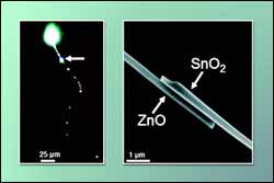
At left a zinc-oxide nanowire laser is pumped with light, which is channeled into a tin-oxide nanoribbon at a junction between the two materials and guided through the rest of the ribbon’s length. At right is an electron microscope image of the junction between wire and ribbon.
Another important step towards realizing the promise of lightning fast photonic technology has been taken by scientists with the U.S. Department of Energy’s Lawrence Berkeley National Laboratory (Berkeley Lab) and the University of California at Berkeley. Researchers have demonstrated that semiconductor nanoribbons, single crystals measuring tens of hundreds of microns in length, but only a few hundred or less nanometers in width and thickness (about one ten-millionth of an inch), can serve as “waveguides” for channeling and directing the movement of light through circuitry.
“Not only have we shown that semiconductor nanoribbons can be used as low-loss and highly flexible optical waveguides, we’ve also shown that they have the potential to be integrated within other active optical components to make photonic circuits,” says Peidong Yang, a chemist with Berkeley Lab’s Materials Sciences Division and a professor with UC Berkeley’s Chemistry Department, who led this research.
The research results of Yang and his team are reported in the August 27, 2004 issue of the journal Science. Co-authoring the paper along with Yang were Matt Law, Donald Sirbuly, Justin Johnson, Josh Goldberger and Richard Saykally, all of whom are with affiliated with Berkeley Lab, UC Berkeley, or both.
In photonic technology, or photonics, the use of electrons moving through semiconductors as information carriers is replaced with the movement of light waves, as measured in units of energy called photons. Whereas electrons must carry information sequentially, one electron at a time, with photons of light there’s virtually no limit to the number of information packets that can simultaneously be transmitted. Call it unparalleled parallel processing.
Hints of the potential of photonics can be glimpsed in today’s fiber-optic communications, where a single optical fiber can carry the equivalent of 300,000 telephone calls at the same time. But the power of fully realized photonics goes far beyond this. For example, it’s been estimated that a photonic internet could transmit data at 160 gigabits per second, which is thousands of times faster than today’s typical high-speed connection. Another possibility is the optical computer, which could solve problems in seconds that would take today’s electronic computers months or even years to solve.
For the promise of photonics to be delivered, however, scientists must first find a way to manipulate and route photons with the same dexterity as they manipulate and route electrons. Whereas other research efforts have successfully experimented with the use of photonic band-gap materials to accomplish this, Yang and his colleagues have focused on the chemical synthesis of nanowires and nanoribbons — they’re like nanotubes only solid throughout rather than hollow inside — that can then be assembled into photonic circuits.
“Chemically synthesized nanowires and nanoribbons have several features that make them good photonic building blocks,” says Yang. “They offer inherent one-dimensionality, a diversity of optical and electrical properties, good size control, low surface roughness and, in principle, the ability to operate above and below light-diffraction limits.”
Yang and his colleagues synthesized their nanoribbon waveguides from tin oxide, a semiconductor of keen technological interest for its exceptional potential for use in transporting both photons and electrons in nanoscale (also referred to as “subwavelength”) components. The single crystalline nanoribbons they produced measured about 1,500 microns in length and featured a variety of widths and thicknesses. Yang says ribbons that measured between 100 to 400 nanometers in width and thickness proved to be ideal for guiding visible and ultraviolet light.
“To steer visible and ultraviolet light within dielectric waveguides, such as the tin oxide crystals we were synthesizing, we needed to make sure that a sufficient portion of the light’s electromagnetic field was confined within the nanostructures so there would be minimal optical transmission loss,” Yang says. “Considering the dielectric constant of the tin oxide, it follows that the diameter of 100 to 400 nanometers would be ideal for waveguiding light that measures from 300 to 800 nanometers in wavelengths.”
In their tests, Yang and his colleagues attached nanowire lasers and optical detectors to opposite ends of their tin oxide nanoribbons, then demonstrated that light could be propagated and modulated through subwavelength optical cavities within the nanoribbons. The nanoribbons were long and strong enough to be pushed, bent, and shaped with the use of a commercial micromanipulator under an optical microscope. Freestanding ribbons were also extremely flexible and could be curved through tight S-turns and twisted into a variety of shapes, which Yang says is “remarkable for a crystal that is brittle in its bulk form.”
Yang also says that while the nanoribbon waveguides can be coupled together to create optical networks that could serve as the basis of miniaturized photonic circuitry, the ribbons need to be in close proximity, preferably in direct physical contact, to enable an efficient transfer of light between them. “We tested various coupling geometries and found that a staggered side-by-side arrangement, in which two ribbons interact over a distance of several micrometers, outperforms direct end-to-end coupling,” Yang says.
The nanoribbon waveguides that Yang and his co-authors report in their Science paper are the newest addition to the growing assortment of nanosized device elements that Yang and his research group have been able to make. Their “toolbox” now includes nanoscale lasers and photodetectors, in addition to the nanoribbon waveguides.
“Ultimately, we would like to integrate all these individual components together into a photonic system-on-a-chip, so that many photonic operations, including light emission, routing, and detection, can be done on a much smaller scale,” says Yang.
Media Contact
More Information:
http://www.lbl.govAll latest news from the category: Power and Electrical Engineering
This topic covers issues related to energy generation, conversion, transportation and consumption and how the industry is addressing the challenge of energy efficiency in general.
innovations-report provides in-depth and informative reports and articles on subjects ranging from wind energy, fuel cell technology, solar energy, geothermal energy, petroleum, gas, nuclear engineering, alternative energy and energy efficiency to fusion, hydrogen and superconductor technologies.


Newest articles

Silicon Carbide Innovation Alliance to drive industrial-scale semiconductor work
Known for its ability to withstand extreme environments and high voltages, silicon carbide (SiC) is a semiconducting material made up of silicon and carbon atoms arranged into crystals that is…

New SPECT/CT technique shows impressive biomarker identification
…offers increased access for prostate cancer patients. A novel SPECT/CT acquisition method can accurately detect radiopharmaceutical biodistribution in a convenient manner for prostate cancer patients, opening the door for more…

How 3D printers can give robots a soft touch
Soft skin coverings and touch sensors have emerged as a promising feature for robots that are both safer and more intuitive for human interaction, but they are expensive and difficult…

