High-performance, single-crystal plastic transistors reveal hidden behavior

Printing circuits on sheets of plastic may offer a low-cost technique for manufacturing thin-film transistors for flexible displays, but maximizing the performance of such devices will require a detailed, fundamental understanding of how charge flows through organic semiconductors.
Now, an unusual way of fabricating single-crystal organic transistors has allowed scientists to probe charge transport within the crystals and to observe a strong anisotropy of the charge transport mobility within the crystal plane never before seen.
“We construct transistors simply by laminating a piece of silicone rubber that supports electrodes and dielectric layers for the transistor – an element that we refer to as a transistor stamp – against the surface of a single crystal,” said John A. Rogers, a professor of materials science and engineering at the University of Illinois at Urbana-Champaign and corresponding author of a paper to appear in the March 12 issue of the journal Science.
“This method separates the synthesis of the crystal from the fabrication of the other elements needed for the transistors,” Rogers said. “It thereby eliminates exposure of the fragile surface of the organic crystals to the hazards of conventional processing.”
The fabrication technique – developed by researchers from Illinois, Rutgers University and Bell Laboratories, Lucent Technologies – not only provides a way to study the physics at the heart of charge transport in these unusual materials, it also has resulted in the highest mobility recorded in an organic semiconductor.
The use of transistor stamps promises to open up the field of basic study of organic semiconductors by allowing devices to be fabricated from pristine organic crystal samples that remain untouched by conventional chemical or mechanical processing.
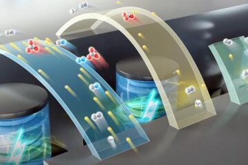
To build their high-performance organic transistors, the researchers start with a simple rubber substrate, upon which they deposit gold films and thin rubber layers to create the gate dielectric and the source, drain and gate electrodes. A high-quality rubrene crystal – grown by the Rutgers group – is then bonded to the substrate to complete assembly. The bonding is performed by a lamination process carried out in ambient conditions without pressure or adhesives.
“While this assembly process could be performed commercially to produce complex circuits, we really designed it to get at the physics,” Rogers said.
“Understanding the fundamental behavior of charge transport in these transistors will help us make better devices for the wide range of electronic applications that are now emerging for these classes of materials.”
As charges flow through conventional thin-film polycrystalline materials, they encounter boundaries between the crystals that disrupt their movement. By studying single crystals, Rogers and his colleagues can eliminate the effects of these grain boundaries and examine the intrinsic transport properties of the crystalline material itself.
“The mobility we measured in these single-crystal devices was about 50 to 100 times larger than in thin-film plastic transistors,” Rogers said. “This result suggests that scattering at grain boundaries is significantly reducing the performance of normal transistors, and points us toward a way of improving these devices.”
Because the bond between stamp and crystal is not permanent, the researchers also can remove the crystal, rotate it, and reattach it to the substrate. Repositioning the crystal allows the scientists to explore the dependence of the mobility on the orientation of the transistor channel relative to the crystal axes.
“We found a huge dependence upon transport direction in the currents that we measured,” Rogers said. “This anisotropy was unexpected, and indicates that transistor performance depends strongly on how the electrodes are oriented relative to the packing of molecules in the crystal.”
The researchers’ findings have clear device implications. In addition to removing grain boundaries, Rogers said, “if you could preferentially order the crystals in these thin films, that would benefit device performance as well.”
Collaborators included Vitaly Podzorov and Michael E. Gershenson at Rutgers, Vikram C. Sundar, Jana Zaumseil, Robert L. Willett and Takao Someya at Bell Labs, and Etienne Menard at Illinois.
The National Science Foundation and the U.S. Department of Energy funded the work.
Media Contact
More Information:
http://www.news.uiuc.edu/news/04/0311crystal.htmlAll latest news from the category: Power and Electrical Engineering
This topic covers issues related to energy generation, conversion, transportation and consumption and how the industry is addressing the challenge of energy efficiency in general.
innovations-report provides in-depth and informative reports and articles on subjects ranging from wind energy, fuel cell technology, solar energy, geothermal energy, petroleum, gas, nuclear engineering, alternative energy and energy efficiency to fusion, hydrogen and superconductor technologies.
Newest articles

High-energy-density aqueous battery based on halogen multi-electron transfer
Traditional non-aqueous lithium-ion batteries have a high energy density, but their safety is compromised due to the flammable organic electrolytes they utilize. Aqueous batteries use water as the solvent for…

First-ever combined heart pump and pig kidney transplant
…gives new hope to patient with terminal illness. Surgeons at NYU Langone Health performed the first-ever combined mechanical heart pump and gene-edited pig kidney transplant surgery in a 54-year-old woman…

Biophysics: Testing how well biomarkers work
LMU researchers have developed a method to determine how reliably target proteins can be labeled using super-resolution fluorescence microscopy. Modern microscopy techniques make it possible to examine the inner workings…


