Low-power tunneling transistor for high-performance devices at low voltage
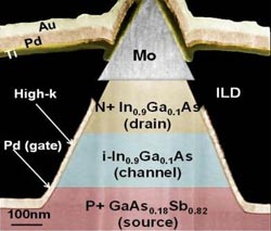
This is a transmission electron microscope cross-section of the vertical TFET. The interface of the source and channel is the point where electron tunneling occurs. ILD is the interlayer dielectric separating the contacts. Top plane contacts are gold (Au), palladium (Pd), and molybdenum (Mo).<br><br>Credit: Suman Datta/Penn State<br>
Called a near broken-gap tunnel field effect transistor (TFET), the new device uses the quantum mechanical tunneling of electrons through an ultrathin energy barrier to provide high current at low voltage.
Penn State, the National Institute of Standards and Technology and IQE, a specialty wafer manufacturer, jointly presented their findings at the International Electron Devices Meeting in Washington, D.C. The IEDM meeting includes representatives from all of the major chip companies and is the recognized forum for reporting breakthroughs in semiconductor and electronic technologies.
Tunnel field effect transistors are considered to be a potential replacement for current CMOS transistors, as device makers search for a way to continue shrinking the size of transistors and packing more transistors into a given area. The main challenge facing current chip technology is that as size decreases, the power required to operate transistors does not decrease in step. The results can be seen in batteries that drain faster and increasing heat dissipation that can damage delicate electronic circuits. Various new types of transistor architecture using materials other than the standard silicon are being studied to overcome the power consumption challenge.
“This transistor has previously been developed in our lab to replace MOSFET transistors for logic applications and to address power issues,” said lead author and Penn State graduate student Bijesh Rajamohanan. “In this work we went a step beyond and showed the capability of operating at high frequency, which is handy for applications where power concerns are critical, such as processing and transmitting information from devices implanted inside the human body.”
For implanted devices, generating too much power and heat can damage the tissue that is being monitored, while draining the battery requires frequent replacement surgery. The researchers, led by Suman Datta, professor of electrical engineering, tuned the material composition of the indium gallium arsenide/gallium arsenide antimony so that the energy barrier was close to zero — or near broken gap, which allowed electrons to tunnel through the barrier when desired. To improve amplification, the researchers moved all the contacts to the same plane at the top surface of the vertical transistor.
This device was developed as part of a larger program sponsored by the National Science Foundation through the Nanosystems Engineering Research Center for Advanced Self-Powered Systems of Integrated Sensors and Technologies (NERC-ASSIST). The broader goal of the ASSIST program is to develop battery-free, body-powered wearable health monitoring systems with Penn State, North Carolina State University, University of Virginia, and Florida International University as participating institutions.
The paper, “Demonstration of InGaAs/GaAsSb Near Broken-gap Tunnel FET with Ion=740µA/µm, GM=700µS/µm and Gigahertz Switching Performance at VDS=0.5V,” will be available in the conference proceedings publication of the IEDM.
Media Contact
More Information:
http://www.psu.eduAll latest news from the category: Power and Electrical Engineering
This topic covers issues related to energy generation, conversion, transportation and consumption and how the industry is addressing the challenge of energy efficiency in general.
innovations-report provides in-depth and informative reports and articles on subjects ranging from wind energy, fuel cell technology, solar energy, geothermal energy, petroleum, gas, nuclear engineering, alternative energy and energy efficiency to fusion, hydrogen and superconductor technologies.


Newest articles

Silicon Carbide Innovation Alliance to drive industrial-scale semiconductor work
Known for its ability to withstand extreme environments and high voltages, silicon carbide (SiC) is a semiconducting material made up of silicon and carbon atoms arranged into crystals that is…

New SPECT/CT technique shows impressive biomarker identification
…offers increased access for prostate cancer patients. A novel SPECT/CT acquisition method can accurately detect radiopharmaceutical biodistribution in a convenient manner for prostate cancer patients, opening the door for more…

How 3D printers can give robots a soft touch
Soft skin coverings and touch sensors have emerged as a promising feature for robots that are both safer and more intuitive for human interaction, but they are expensive and difficult…

