Growing nanowires horizontally yields new benefit: 'nano-LEDs'
Nanowires typically are “grown” by the controlled deposition of molecules—zinc oxide, for example—from a gas onto a base material, a process called chemical vapor deposition (CVD). Most CVD techniques form nanowires that rise vertically from the surface like brush bristles.
Because the wire only contacts the substrate at one end, it tends not to share characteristics with the substrate material—a less-than-preferred trait because the exact composition of the nanowire will then be hard to define. Vertical growth also produces a dense forest of nanowires, making it difficult to find and re-position individual wires of superior quality.
To remedy these shortcomings, NIST chemists Babak Nikoobakht and Andrew Herzing developed a “surface-directed” method for growing nanowires horizontally across the substrate (see “NIST Demos Industrial-Grade Nanowire Device Fabrication” NIST Tech Beat, Oct. 25, 2007, at http://www.nist.gov/public_affairs/techbeat/tb2007_1025.htm#nanowire).
Like many vertical growth CVD methods, the NIST fabrication technique uses gold as a catalyst for crystal formation. The difference is that the gold deposited in the NIST method is heated to 900 degrees Celsius (1,652 degrees Fahrenheit), converting it to a nanoparticle that serves as growth site and medium for the crystallization of zinc oxide molecules. As the zinc oxide nanocrystal grows, it pushes the gold nanoparticle along the surface of the substrate (in this experiment, gallium nitride) to form a nanowire that grows horizontally across the substrate and so exhibits properties strongly influenced by its base material.
In recent work published in ACS Nano,* Nikoobakht and Herzing increased the thickness of the gold catalyst nanoparticle from less than 8 nanometers to approximately 20 nanometers. The change resulted in nanowires that grew a secondary structure, a shark-like “dorsal fin” (referred to as a “nanowall”) where the zinc oxide portion is electron-rich and the gallium nitride portion is electron-poor. The interface between these two materials—known as a p-n heterojunction—allows electrons to flow across it when the nanowire-nanowall combination was charged with electricity. In turn, the movement of electrons produced light and led the researchers to dub it a “nano LED.”
Unlike previous techniques for producing heterojunctions, the NIST “surface-directed” fabrication method makes it easy to locate individual heterojunctions on the surface. This feature is especially useful when a large number of heterojunctions must be grouped in an array so that they can be electrically charged as a light-emitting unit.
Transmission electron microscope (TEM) examination of the zinc oxide-gallium nitride nanowires and nanowalls revealed few structural defects in the nanowires and very distinct p-n heterojunctions in the nanowalls, both affirmations of the effectiveness of the NIST “surface directed” fabrication method.
Nikoobakht and Herzing hope to improve the nano LEDs in future experiments using better geometry and material designs, and then apply them in the development of light sources and detectors useful in photonic devices or lab-on-a-chip platforms.
* B. Nikkoobakht and A. Herzing. Formation of planar arrays of one-dimensional p-n heterojunctions using surface-directed growth of nanowires and nanowalls. ACS Nano. Published online Sept. 15, 2010
Media Contact
More Information:
http://www.nist.govAll latest news from the category: Power and Electrical Engineering
This topic covers issues related to energy generation, conversion, transportation and consumption and how the industry is addressing the challenge of energy efficiency in general.
innovations-report provides in-depth and informative reports and articles on subjects ranging from wind energy, fuel cell technology, solar energy, geothermal energy, petroleum, gas, nuclear engineering, alternative energy and energy efficiency to fusion, hydrogen and superconductor technologies.


Newest articles
Bringing bio-inspired robots to life
Nebraska researcher Eric Markvicka gets NSF CAREER Award to pursue manufacture of novel materials for soft robotics and stretchable electronics. Engineers are increasingly eager to develop robots that mimic the…
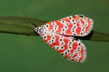
Bella moths use poison to attract mates
Scientists are closer to finding out how. Pyrrolizidine alkaloids are as bitter and toxic as they are hard to pronounce. They’re produced by several different types of plants and are…
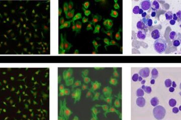
AI tool creates ‘synthetic’ images of cells
…for enhanced microscopy analysis. Observing individual cells through microscopes can reveal a range of important cell biological phenomena that frequently play a role in human diseases, but the process of…

