Breakthrough to the development of energy-saving devices for the next generation
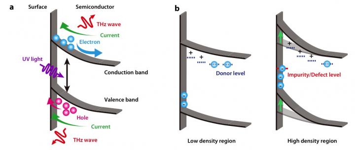
As shown in Figure a, in the neighborhood of the surface of semiconductor of GaN, the energy band is bent due to the surface potential. It is thought that photoexcited carriers are accelerated by the band bending, thereby radiating THz. It is also thought that the change in THz wave emission intensity due to defects, as shown in Figure b, is because the energy band bent significantly due to electrons trapped by defects near the surface, which further accelerated carriers. This shows that LTEM is effective for measuring the defect density of the surface of wide-gap semiconductors and their distribution of the surface potential. Credit: Osaka University
Wide-gap semiconductors such as gallium nitride (GaN) are widely used for optical devices such as blue LED and are also anticipated as materials for next-generation energy saving power devices and solar cells.
However, the quality of GaN crystals does not come up to that of conventional semiconductor materials such as silicon (Si) and this prevents GaN from being used for power devices.
For that reason, the establishment of technology for producing high-quality crystals with fewer defects and rearrangement is expected, and the development of a new evaluation technology is crucial.
A group of researchers led by Iwao Kawayama, an associate professor of the Institute of Laser Engineering at Osaka University, in cooperation with Screen Holdings Co., Ltd., succeeded in visualizing changes in defect density on the surface of GaN through the laser terahertz emission microscope (LTEM) which measures THz waves generated by laser emission.
This group's discovery shows that LTEM is useful as a new method for evaluating the quality of wide-gap semiconductors and it is also expected that LTEM will bring a breakthrough in the development of next-generation optical devices, super high frequency devices, and energy devices.
The group examined the intensity distribution of THz generated by radiating ultraviolet femtosecond laser pulses on the surface of GaN crystal through LTEM.
As a result, it was found that there were regions with high intensity of THz emission and ones with low intensity of THz emission.
Additionally, when the LTEM image was compared with the image obtained through photoluminescence (PL) using a conventional method, it was found that there was a strong correlation between the distribution of emission intensity due to lattice defects and the intensity distribution of THz wave emission.
Furthermore, from results measurement through modification of excited lasers, it was confirmed that THz emission needs excitation light with larger energy than the band gap energy.
###
This research was featured in the electronic version of Scientific Reports (UK) on September 9, 2015.
Media Contact
All latest news from the category: Power and Electrical Engineering
This topic covers issues related to energy generation, conversion, transportation and consumption and how the industry is addressing the challenge of energy efficiency in general.
innovations-report provides in-depth and informative reports and articles on subjects ranging from wind energy, fuel cell technology, solar energy, geothermal energy, petroleum, gas, nuclear engineering, alternative energy and energy efficiency to fusion, hydrogen and superconductor technologies.


Newest articles

Silicon Carbide Innovation Alliance to drive industrial-scale semiconductor work
Known for its ability to withstand extreme environments and high voltages, silicon carbide (SiC) is a semiconducting material made up of silicon and carbon atoms arranged into crystals that is…

New SPECT/CT technique shows impressive biomarker identification
…offers increased access for prostate cancer patients. A novel SPECT/CT acquisition method can accurately detect radiopharmaceutical biodistribution in a convenient manner for prostate cancer patients, opening the door for more…

How 3D printers can give robots a soft touch
Soft skin coverings and touch sensors have emerged as a promising feature for robots that are both safer and more intuitive for human interaction, but they are expensive and difficult…

