Self-assembled nanowires could make chips smaller and faster
In a paper to appear in the IEEE (Institute of Electrical and Electronics Engineers) journal Electron Device Letters, U. of I. electrical and computer engineering professor Xiuling Li and graduate research assistant Seth Fortuna describe the first metal-semiconductor field-effect transistor fabricated with a self-assembled, planar gallium-arsenide nanowire channel.
Nanowires are attractive building blocks for both electronics and photonics applications. Compound semiconductor nanowires, such as gallium arsenide, are especially desirable because of their better transport properties and versatile heterojunctions. However, a number of challenges – including integration with existing microelectronics – must first be overcome.
“Our new planar growth process creates self-aligned, defect-free gallium-arsenide nanowires that could readily be scaled up for manufacturing purposes,” said Li, who also is affiliated with the university's Micro and Nanoelectronics Laboratory and the Beckman Institute. “It's a non-lithographic process that can precisely control the nanowire dimension and orientation, yet is compatible with existing circuit design and fabrication technology.”
The gallium-arsenide nanowire channel used in the researchers' demonstration transistor was grown by metal organic chemical vapor deposition using gold as a catalyst. The rest of the transistor was made with conventional microfabrication techniques.
While the diameter of the transistor's nanowire channel was approximately 200 nanometers, nanowires with diameters as small as 5 nanometers can be made with the gold-catalyzed growth technique, the researchers report. The self-aligned orientation of the nanowires is determined by the crystal structure of the substrate and certain growth parameters.
In earlier work, Li and Fortuna demonstrated they could grow the nanowires and then transfer-print them on other substrates, including silicon, for heterogeneous integration. “Transferring the self-aligned planar nanowires while maintaining both their position and alignment could enable flexible electronics and photonics at a true nanometer scale,” the researchers wrote in the December 2008 issue of the journal Nano Letters.
In work presented in the current paper, the researchers grew the gallium-arsenide nanowire channel in place, instead of transferring it. In contrast to the common types of non-planar gallium arsenide nanowires, the researchers' planar nanowire was free from twin defects, which are rotational defects in the crystal structure that decrease the mobility of the charge carriers.
“By replacing the standard channel in a metal-semiconductor field-effect transistor with one of our planar nanowires, we demonstrated that the defect-free nanowire's electron mobility was indeed as high as the corresponding bulk value,” Fortuna said. “The high electron mobility nanowire channel could lead to smaller, better and faster devices.”
Considering their planar, self-aligned and transferable nature, the nanowire channels could help create higher performance transistors for next-generation integrated circuit applications, Li said.
The high quality planar nanowires can also be used in nano-injection lasers for use in optical communications.
The researchers are also developing new device concepts driven by further engineering of the planar one-dimensional nanostructure.
The work was supported by the National Science Foundation.
Media Contact
More Information:
http://www. illinois.eduAll latest news from the category: Power and Electrical Engineering
This topic covers issues related to energy generation, conversion, transportation and consumption and how the industry is addressing the challenge of energy efficiency in general.
innovations-report provides in-depth and informative reports and articles on subjects ranging from wind energy, fuel cell technology, solar energy, geothermal energy, petroleum, gas, nuclear engineering, alternative energy and energy efficiency to fusion, hydrogen and superconductor technologies.


Newest articles
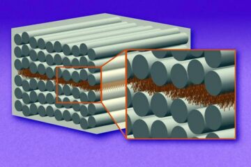
“Nanostitches” enable lighter and tougher composite materials
In research that may lead to next-generation airplanes and spacecraft, MIT engineers used carbon nanotubes to prevent cracking in multilayered composites. To save on fuel and reduce aircraft emissions, engineers…
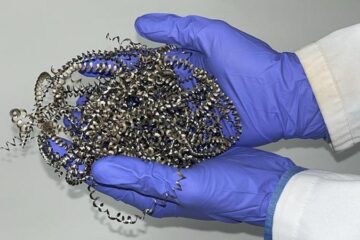
Trash to treasure
Researchers turn metal waste into catalyst for hydrogen. Scientists have found a way to transform metal waste into a highly efficient catalyst to make hydrogen from water, a discovery that…
Real-time detection of infectious disease viruses
… by searching for molecular fingerprinting. A research team consisting of Professor Kyoung-Duck Park and Taeyoung Moon and Huitae Joo, PhD candidates, from the Department of Physics at Pohang University…

