University of Illinois researchers create 1-step graphene patterning method
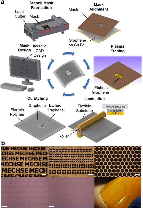
a) This is a schematic illustration of the one-step polymer-free approach to fabricate patterned graphene on a flexible substrate. A stencil mask is designed by computer-aided design software and fabricated by a laser cutter. The fabricated mask is aligned on the as-grown CVD graphene on a Cu foil, and the exposed graphene region is removed by oxygen plasma. The patterned graphene is laminated onto a flexible substrate, followed by etching of the copper foil. b) Optical microscope images and photographs of various stencil masks with sophisticated micro-scale features (top row) and corresponding graphene array patterns transferred onto SiO2 substrate and flexible Kapton film (bottom row). All scale bars: 300 μm. Credit: University of Illinois
Graphene, a two-dimensional carbon allotrope, has received immense scientific and technological interest. Combining exceptional mechanical properties, superior carrier mobility, high thermal conductivity, hydrophobicity, and potentially low manufacturing cost, graphene provides a superior base material for next generation bioelectrical, electromechanical, optoelectronic, and thermal management applications.
“Significant progress has been made in the direct synthesis of large-area, uniform, high quality graphene films using chemical vapor deposition (CVD) with various precursors and catalyst substrates,” explained SungWoo Nam, an assistant professor of mechanical science and engineering at Illinois.
“However, to date, the infrastructure requirements on post-synthesis processing–patterning and transfer–for creating interconnects, transistor channels, or device terminals have slowed the implementation of graphene in a wider range of applications.”
“In conjunction with the recent evolution of additive and subtractive manufacturing techniques such as 3D printing and computer numerical control milling, we developed a simple and scalable graphene patterning technique using a stencil mask fabricated via a laser cutter,” stated Keong Yong, a graduate student and first author of the paper, “Rapid Stencil Mask Fabrication Enabled One-Step Polymer-Free Graphene Patterning and Direct Transfer for Flexible Graphene Devices appearing in Scientific Reports.
“Our approach to patterning graphene is based on a shadow mask technique that has been employed for contact metal deposition,” Yong added. “Not only are these stencil masks easily and rapidly manufactured for iterative rapid prototyping, they are also reusable, enabling cost-effective pattern replication. And since our approach involves neither a polymeric transfer layer nor organic solvents, we are able to obtain contamination-free graphene patterns directly on various flexible substrates.”
Nam stated that this approach demonstrates a new possibility to overcome limitations imposed by existing post-synthesis processes to achieve graphene micro-patterning. Yong envisions this facile approach to graphene patterning sets forth transformative changes in “do It yourself” (DIY) graphene-based device development for broad applications including flexible circuits/devices and wearable electronics.
“This method allows rapid design iterations and pattern replications, and the polymer-free patterning technique promotes graphene of cleaner quality than other fabrication techniques,” Nam said. “We have shown that graphene can be patterned into varying geometrical shapes and sizes, and we have explored various substrates for the direct transfer of the patterned graphene.”
###
In addition to Nam and Yong, study co-authors include Ali Ashraf and Pilgyu Kang from the Department of Mechanical Science and Engineering at Illinois.
Media Contact
All latest news from the category: Materials Sciences
Materials management deals with the research, development, manufacturing and processing of raw and industrial materials. Key aspects here are biological and medical issues, which play an increasingly important role in this field.
innovations-report offers in-depth articles related to the development and application of materials and the structure and properties of new materials.


Newest articles

Silicon Carbide Innovation Alliance to drive industrial-scale semiconductor work
Known for its ability to withstand extreme environments and high voltages, silicon carbide (SiC) is a semiconducting material made up of silicon and carbon atoms arranged into crystals that is…

New SPECT/CT technique shows impressive biomarker identification
…offers increased access for prostate cancer patients. A novel SPECT/CT acquisition method can accurately detect radiopharmaceutical biodistribution in a convenient manner for prostate cancer patients, opening the door for more…

How 3D printers can give robots a soft touch
Soft skin coverings and touch sensors have emerged as a promising feature for robots that are both safer and more intuitive for human interaction, but they are expensive and difficult…

