Unique anti-reflective and self-cleaning plastic films to be ramped up for industry use

Fast, high-volume production of plastics with specially engineered surfaces will soon be available using a cheaper and simpler method. IMRE and its Industrial Consortium On Nanoimprint (ICON) partner companies are piloting roll-to-roll nanoimprint technology to mass produce two types of patterned nanoimprinted plastic films.
These are films with low reflectivity and better viewing angles, as well as durable, scratch-resistant films with ‘self-cleaning’ surfaces. This technology can be more cost effective than conventional batch production as ICON uses roll-to-roll processing, which enables the continuous, high throughput production of such materials on a large scale. Potential applications of such mass-produced anti-reflective films are in the mobile device and tablet markets while the self-cleaning plastics can be applied to surfaces such as walls of buildings.
IMRE and five companies, namely, Innox Higa Singapore Pte Ltd, Micro Resist Technology GmbH, NTT Advanced Technology, SABIC Innovative Plastics and Solves Innovative Technology will work together to develop the materials and scale up production of the films. Nanoimprinting technology involves creating arrays of very tiny, nano-sized surfaces to form unique patterns that give the surfaces certain properties such as low reflectivity, super-hydrophobicity (water repelling), non-sticky adhesiveness or anti-bacteria qualities.
In this collaboration, the partners are developing tougher resins for the nanostructures that are then patterned onto the plastics via IMRE’s unique nanopatterning processes. The process is then easily scaled up using ultraviolet roll-to-roll nanoimprinters so that the films can be used in eventual prototyping on surfaces and devices.
“The partnership with industries to advance the technology towards scale-up will bring nanoimprinting technology a step closer to full industry adoption,” said IMRE scientist Dr Low Hong Yee adding that one of the goals of ICON has been to nurture nanoimprint technology from a primarily laboratory-based process to one with industrial manufacturing and consumer application potential.
“Nanoimprinting is a very versatile and extraordinary technology that turns ordinary surfaces into functional ones. It is also encouraging to see the translation from science to large-scale manufacturing in such a short span of time,” said Prof Andy Hor, Executive Director of IMRE.
“We are a company that specialises in photoresists and polymers for micro and nanolithography. Within the ICON project, we will provide tailor-made polymer materials for nanostructured functional films. It is a unique opportunity for us to adapt materials specifically for roll-to-roll processes as well as for “hard” industrial requirements which cannot be achieved by today’s off-the-shelf materials. This will strengthen Micro Resist Technology’s market business prospects as global supplier of materials for next-generation lithography and nanolithography,” said Dr Marko Vogler, Business Unit Manager, Nanoimprint Materials and Hybrid Polymers, Micro Resist Technology GmbH, Germany.
“SABIC Innovative Plastics is excited to be part of this ICON project. It is a unique platform provided by IMRE for us to access advanced nanoimprint technology and enhance our core competencies to provide innovative solutions to our customers and end users in various market segments,” said Dr Mahari Tjahjadi, Technology Director, Specialty Film & Sheet, SABIC Innovative Plastics.
“This is a very exciting time for us from the perspective of a local company. Since being involved in the pioneering development of cutting edge technology can put us on the global map, Solves is ready to support mass production using nanoimprint technology!” said Mr Koh Teng Hwee, Managing Director of Solves Innovative Technology, a local small and medium enterprise (SME) that helped co-develop the UV roll-to-roll tool with the IMRE team.
The pilot manufacturing project will last a year after which the consortium can further develop and market the technology.
For media enquiries, please contact:
Mr Eugene Low
Manager, Corporate Communications
for Institute of Materials Research and Engineering (IMRE)
3, Research Link
Singapore 117602
DID +65 6874 8491
Mobile +65 9230 9235
Email loweom@scei.a-star.edu.sg
For technical enquiries, please contact:
Dr Jaslyn Law
Scientist II
Institute of Materials Research and Engineering (IMRE)
3, Research Link
Singapore 117602
DID +65 6874 7902
E-mail lawj@imre.a-star.edu.sg
ANNEX A – A*STAR Corporate Profiles
About the Institute of Materials Research and Engineering (IMRE)
The Institute of Materials Research and Engineering (IMRE) is a research institute of the Agency for Science, Technology and Research (A*STAR). The Institute has capabilities in materials analysis & characterisation, design & growth, patterning & fabrication, and synthesis & integration. We house a range of state-of-the-art equipment for materials research including development, processing and characterisation. IMRE conducts a wide range of research, which includes novel materials for organic solar cells, photovoltaics, printed electronics, catalysis, bio-mimetics, microfluidics, quantum dots, heterostructures, sustainable materials, atom technology, etc. We collaborate actively with other research institutes, universities, public bodies, and a wide spectrum of industrial companies, both globally and locally.
About the Agency for Science, Technology and Research (A*STAR)
The Agency for Science, Technology and Research (A*STAR) is the lead agency for fostering world-class scientific research and talent for a vibrant knowledge-based and innovation-driven Singapore. A*STAR oversees 14 biomedical sciences and physical sciences and engineering research institutes, and six consortia & centres, located in Biopolis and Fusionopolis as well as their immediate vicinity.
A*STAR supports Singapore's key economic clusters by providing intellectual, human and industrial capital to its partners in industry. It also supports extramural research in the universities, hospitals, research centres, and with other local and international partners.
ANNEX B – More information on ICON and nanoimprint technology
About nanoimprint technology and ICON
Nanoimprint technology produces nanometer-sized structures of greater complexity using fewer processing steps, while minimising wastage of materials. It has evolved from a lithography technology for the semiconductor industry to a platform process technology that can be adapted to a wide range of applications. The Industrial Consortium On Nanoimprint (ICON) is Singapore’s first nanotechnology consortium that encourages companies to adopt versatile, industry-ready nanoimprinting technology that can bring products to the market through sustainable manufacturing. The members of ICON will gain first-hand access to these new technologies by working on joint projects to develop new products and applications that can potentially have huge savings in R&D.
Under ICON, three projects have been successfully launched since August 2010. This is the fourth project in ICON on the topic of large area functional film and in collaboration with Innox Higa Singapore Pte Ltd, Micro Resist Technology GmbH, NTT Advanced Technology, SABIC Innovative Plastics, and Solves Innovative Technology.
Media Contact
All latest news from the category: Materials Sciences
Materials management deals with the research, development, manufacturing and processing of raw and industrial materials. Key aspects here are biological and medical issues, which play an increasingly important role in this field.
innovations-report offers in-depth articles related to the development and application of materials and the structure and properties of new materials.
Newest articles

Superradiant atoms could push the boundaries of how precisely time can be measured
Superradiant atoms can help us measure time more precisely than ever. In a new study, researchers from the University of Copenhagen present a new method for measuring the time interval,…

Ion thermoelectric conversion devices for near room temperature
The electrode sheet of the thermoelectric device consists of ionic hydrogel, which is sandwiched between the electrodes to form, and the Prussian blue on the electrode undergoes a redox reaction…
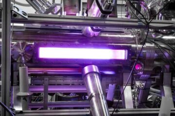
Zap Energy achieves 37-million-degree temperatures in a compact device
New publication reports record electron temperatures for a small-scale, sheared-flow-stabilized Z-pinch fusion device. In the nine decades since humans first produced fusion reactions, only a few fusion technologies have demonstrated…


