New spintronics material could help usher in next generation of microelectronics
As the electronics industry works toward developing smaller and more compact devices, the need to create new types of scaled-down semiconductors that are more efficient and use less power has become essential.
In a study to be published in the April issue of Nature Materials (currently available online), researchers from UCLA's Henry Samueli School of Engineering and Applied Science describe the creation of a new material incorporating spintronics that could help usher in the next generation of smaller, more affordable and more power-efficient devices.
While conventional complementary metal-oxide semiconductors (CMOS), a technology used today in all types of electronics, rely on electrons' charge to power devices, the emerging field of spintronics exploits another aspect of electrons — their spin, which could be manipulated by electric and magnetic fields.
“With the use of nanoscaled magnetic materials, spintronics or electronic devices, when switched off, will not have a stand-by power dissipation problem. With this advantage, devices with much lower power consumption, known as non-volatile electronics, can become a reality,” said the study's corresponding author, Kang L. Wang, Raytheon Professor of Electrical Engineering at UCLA Engineering, whose team carried out the research. “Our approach provides a possible solution to address the critical challenges facing today's microelectronics industry and sheds light on the future of spintronics.”
“We've built a new class of material with magnetic properties in a dilute magnetic semiconductor (DMS) system,” said Faxian Xiu, a UCLA senior researcher and lead author of the study. “Traditionally, it's been really difficult to enhance the ferromagnetism of this material above room temperature. However in our work, by using a type of quantum structure, we've been able to push the ferromagnetism above room temperature.”
Ferromagnetism is the phenomenon by which certain materials form permanent magnets. In the past, the control of magnetic properties has been accomplished by applying an electric current. For example, passing an electric current will generate magnetic fields. Unfortunately, using electric currents poses significant challenges for reducing power consumption and for device miniaturization.
“You can think of a transformer, which passes a current to generate a magnetic field. This will have huge power dissipation (heat),” Xiu said. “In our study, we tried to modulate the magnetic properties of DMS without passing the current.”
Ferromagnetic coupling in DMS systems, the researchers say, could lead to a new breed of magneto-electronic devices that alleviate the problems related to electric currents. The electric field–controlled ferromagnetism reported in this study shows that without passing an electric current, electronic devices could be operated and functioning based on the collective spin behavior of the carriers. This holds great promise for building next-generation nanoscaled integrated chips with much lower power consumption.
To achieve the ferromagnetic properties, Kang's group grew germanium dots on a silicon p-type substrate, creating quantum dots on top of the substrate. Silicon and germanium are ideal candidates because of their excellent compatibility and ability to be incorporated within conventional CMOS technology. The quantum dots, which are themselves semiconductors, would then be utilized in building new devices.
“To demonstrate possible applications of these fantastic quantum dots, we fabricated metal-oxide semiconductor devices and used these dots as the channel layer. By applying an electric field, we are able to control the hole concentration inside the dots and thus modulate their ferromagnetism,” Xiu said.
“This finding is significant in the sense that it opens up a completely new paradigm for next-generation microelectronics, which takes advantage of the spin properties of carriers, in addition to the existing charge transport as envisaged in the conventional CMOS technology.”
The key is to be able to use this material at room temperature.
“The material is not very useful if it doesn't work at room temperature,” Wang said. “We want to be able to use it anywhere. In this work, we've achieved success on electric field–controlled ferromagnetism at 100 degrees Kelvin and are moving towards room temperature. We feel strongly that we'll be able to accomplish this. Once we've achieved room-temperature controllability, we'll be able to start building real devices to demonstrate its viability in non-volatile electronic devices.”
Study collaborators Jin Zou, professor of material engineering, and postdoctoral fellow Yong Wang, both from the University of Queensland, Australia, also contributed significantly to this work.
The study was funded by the Center for Functional Engineered Nano Architectronics (FENA), the Western Institute of Nanoelectronics (WIN) at UCLA Engineering, and in part by Intel Corp. and the Australian government.
The UCLA Henry Samueli School of Engineering and Applied Science, established in 1945, offers 28 academic and professional degree programs, including an interdepartmental graduate degree program in biomedical engineering. Ranked among the top 10 engineering schools at public universities nationwide, the school is home to eight multimillion-dollar interdisciplinary research centers in wireless sensor systems, nanotechnology, nanomanufacturing and nanoelectronics, all funded by federal and private agencies.
For more news, visit the UCLA Newsroom and follow us on Twitter.
Media Contact
More Information:
http://www.ucla.eduAll latest news from the category: Materials Sciences
Materials management deals with the research, development, manufacturing and processing of raw and industrial materials. Key aspects here are biological and medical issues, which play an increasingly important role in this field.
innovations-report offers in-depth articles related to the development and application of materials and the structure and properties of new materials.


Newest articles
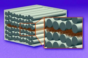
“Nanostitches” enable lighter and tougher composite materials
In research that may lead to next-generation airplanes and spacecraft, MIT engineers used carbon nanotubes to prevent cracking in multilayered composites. To save on fuel and reduce aircraft emissions, engineers…
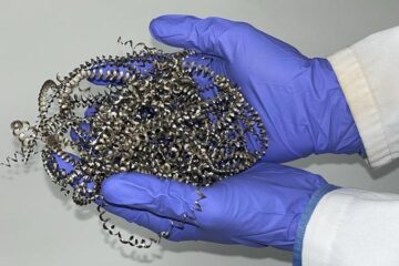
Trash to treasure
Researchers turn metal waste into catalyst for hydrogen. Scientists have found a way to transform metal waste into a highly efficient catalyst to make hydrogen from water, a discovery that…
Real-time detection of infectious disease viruses
… by searching for molecular fingerprinting. A research team consisting of Professor Kyoung-Duck Park and Taeyoung Moon and Huitae Joo, PhD candidates, from the Department of Physics at Pohang University…

