Just Scratching the Surface: New Technique Maps Nanomaterials as They Grow
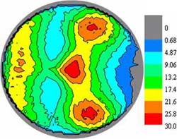
Rensselaer/Gwo-Ching Wang <br>The new technique maps the surface of a nanomaterial as it grows. In this figure, a surface pole figure has been created for magnesium nanoblades.
“Since we discovered this technique, we have been trying to get the word out to the nanoscience and nanotechnology research community,” said professor and head of physics, applied physics, and astronomy Gwo-Ching Wang, who helped discover the technique.
“It is inexpensive because it uses existing technology and vastly increases the rate of discovery by giving researchers a very clear picture of how to perfect and duplicate the growth of a new nanomaterial without spending months characterizing its structures after the growth.”
The approach is based on a commonly used technique known as reflection high-energy electron diffraction, or RHEED. The traditional RHEED system creates an interference pattern of the surface of the nanomaterial. The pattern contains only partial information of the surface and is only a snapshot in time of the growing surface. The researchers modified the traditional RHEED technique by rotating the substrate on which the nanomaterial is being grown. This gives them a diagram containing the complete information on the crystal orientation distribution of the growing surface.
The new technique is different from other common techniques such as X-rays because it monitors the surface structure of the material as it grows. X-ray and other technologies measure the entire material, from the tip of the new growth straight through the substrate that the material is growing on. The new RHEED technique shows the growth of only a few nanometers of a material at a time.
“The creation of a surface crystal orientation diagram is particularly important for revealing the nature of the growth of nanostructures such as nanodots, nanorods, and nanoblades, which have strong energy and data storage capabilities, but their orientation can change dramatically over time,” Wang said. These changes in crystal orientation and morphology of the material can substantially increase or decrease the material’s efficiency. It also makes their use in consumer products difficult because of their unpredictability, according to Wang.
Wang views solar energy materials as one of the most important applications for the new technique. The most efficient solar panels on the market are comprised of single crystal materials, meaning that the material is one unbroken material with no grain boundaries. Grain boundaries in a nanomaterial cause huge decreases in energy-conversion capabilities. But, single crystal solar cells are so costly that they could never be widely used on the consumer market, Wang said. So, many scientists and solar cell companies are working to create polycrystalline materials that grow in such a way that they transfer light into electricity similar to a single crystal material despite having grain boundaries. These materials are also much less expensive, according to Wang.
“The problem with creating high-quality polycrystalline materials is that you need a powerful technique to monitor them in nanoscale dimensions as they grow so you can quickly work on recreating the material to maximize its efficiency,” Wang said. “The new RHEED technique really allows researchers to create a material, see how it formed, and then turn around and recreate the most ideal version of that material without extensive experimentations.”
Wang was joined in her research by Toh-Ming Lu, professor of physics, applied physics, and astronomy, and postdoctoral research associate Fu Tang. Together they have presented their findings within the Proceedings of SPIE and the Journal of Physics D: Applied Physics as well as at conferences around the world including the American Vacuum Society 55th International Symposium and Exhibition on Oct. 23 and before representatives from the Department of Energy on Oct. 31.
“Everywhere we go to present these findings, people have become more and more excited about the possibilities that it opens up for them in their own research,” she said.
Media Contact
More Information:
http://www.rpi.eduAll latest news from the category: Materials Sciences
Materials management deals with the research, development, manufacturing and processing of raw and industrial materials. Key aspects here are biological and medical issues, which play an increasingly important role in this field.
innovations-report offers in-depth articles related to the development and application of materials and the structure and properties of new materials.


Newest articles

Silicon Carbide Innovation Alliance to drive industrial-scale semiconductor work
Known for its ability to withstand extreme environments and high voltages, silicon carbide (SiC) is a semiconducting material made up of silicon and carbon atoms arranged into crystals that is…

New SPECT/CT technique shows impressive biomarker identification
…offers increased access for prostate cancer patients. A novel SPECT/CT acquisition method can accurately detect radiopharmaceutical biodistribution in a convenient manner for prostate cancer patients, opening the door for more…

How 3D printers can give robots a soft touch
Soft skin coverings and touch sensors have emerged as a promising feature for robots that are both safer and more intuitive for human interaction, but they are expensive and difficult…

