Scientists reveal the fundamental limitation in the key material for solid-state lighting
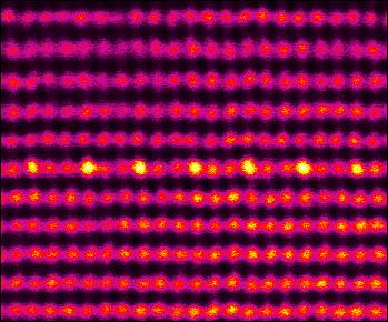
This is a scanning transmission electron microscopy image of the atomic ordering in (In, Ga)N monolayer: single atomic column, containing only indium (In) atoms (shown by higher intensity on the image), followed by two, containing only gallium (Ga) atoms. Credit: IKZ Berlin
Despite the progress in the field of green LEDs and lasers, the researchers could not overcome the limit of 30% of indium content in the films. The reason for that was unclear up to now: is it a problem of finding the right growth conditions or rather a fundamental effect that cannot be overcome? Now, an international team from Germany, Poland and China has shed new light on this question and revealed the mechanism responsible for that limitation.
In their work the scientists tried to push the indium content to the limit by growing single atomic layers of InN on GaN. However, independent on growth conditions, indium concentrations have never exceeded 25% – 30% – a clear sign of a fundamentally limiting mechanism.
The researchers used advanced characterization methods, such as atomic resolution transmission electron microscope (TEM) and in-situ reflection high-energy electron diffraction (RHEED), and discovered that, as soon as the indium content reaches around 25 %, the atoms within the (In, Ga)N monolayer arrange in a regular pattern – single atomic column of In alternates with two atomic columns of Ga atoms.
Comprehensive theoretical calculations revealed that the atomic ordering is induced by a particular surface reconstruction: indium atoms are bonded with four neighboring atoms, instead of expected three. This creates stronger bonds between indium and nitrogen atoms, which, on one hand, allows to use higher temperatures during the growth and provides material with better quality. On the other hand, the ordering sets the limit of the In content of 25%, which cannot be overcome under realistic growth conditions.
“Apparently, a technological bottleneck hampers all the attempts to shift the emission from the green towards the yellow and the red regions of the spectra. Therefore, new original pathways are urgently required to overcome these fundamental limitations,” states Dr. Tobias Schulz, scientist at the Leibniz-Institut fuer Kristallzuechtung; “for example, growth of InGaN films on high quality InGaN pseudo-substrates that would reduce the strain in the growing layer.”
However, the discovery of ordering may help to overcome well known limitations of the InGaN material system: localization of charge carriers due to fluctuations in the chemical composition of the alloy. Growing stable ordered (In, Ga)N alloys with the fixed composition at high temperatures could thus improve the optical properties of devices.
###
The work is a result of a collaboration between Leibniz-Institut fuer Kristallzuechtung (Berlin, Germany), Max-Planck-Institut fuer Eisenforschung (Duesseldorf, Germany), Paul-Drude Institut fuer Festkoerperelektronik (Berlin, Germany), Institute of High-Pressure Physics (Warsaw, Poland), and State Key Laboratory of Artificial Microstructure and Mesoscopic Physics (Beijing, China).
Media Contact
All latest news from the category: Materials Sciences
Materials management deals with the research, development, manufacturing and processing of raw and industrial materials. Key aspects here are biological and medical issues, which play an increasingly important role in this field.
innovations-report offers in-depth articles related to the development and application of materials and the structure and properties of new materials.


Newest articles

Silicon Carbide Innovation Alliance to drive industrial-scale semiconductor work
Known for its ability to withstand extreme environments and high voltages, silicon carbide (SiC) is a semiconducting material made up of silicon and carbon atoms arranged into crystals that is…

New SPECT/CT technique shows impressive biomarker identification
…offers increased access for prostate cancer patients. A novel SPECT/CT acquisition method can accurately detect radiopharmaceutical biodistribution in a convenient manner for prostate cancer patients, opening the door for more…

How 3D printers can give robots a soft touch
Soft skin coverings and touch sensors have emerged as a promising feature for robots that are both safer and more intuitive for human interaction, but they are expensive and difficult…

