Scientists fashion semiconductors into flexible membranes
University of Wisconsin-Madison researchers have demonstrated a way to release thin membranes of semiconductors from a substrate and transfer them to new surfaces-an advance that could unite the properties of silicon and many other materials, including diamond, metal and even plastic.
Led by materials science and engineering graduate student Michelle Roberts, the team reports in the April 9 issue of Nature Materials that the freed membranes, just tens of nanometers thick, retain all the properties of silicon in wafer form. Yet, the nanomembranes are flexible, and by varying the thicknesses of the silicon and silicon-germanium layers composing them, scientists can make membrane shapes ranging from flat to curved to tubular.
Most importantly, the technique stretches the nanomembranes in a predictable and easily controlled manner, says materials science and engineering professor Max Lagally, who is Roberts’ advisor. In silicon that is stretched, or under tensile strain, current flows faster-a fact engineers already exploit to help control silicon’s conductivity and produce speedier electronics. Strain also becomes important whenever different materials are integrated.
The new technique makes tuning the strain of materials simpler, while avoiding the defects that normally result. In addition, Lagally says: “We’re no longer held to a rigid rock of material. We now have the ability to transfer the membranes to anything we want. So, there are some really novel things we can do.”
Potential applications, he says, include flexible electronic devices, faster transistors, nano-size photonic crystals that steer light, and lightweight sensors for detecting toxins in the environment or biological events in cells.
Although it could make controlling strain easier, the technique is not manufacturing-ready, cautions physics professor Mark Eriksson, because it requires the release of nanomembranes into solution before bonding to other materials.
“What we’ve done is a first demonstration,” says Eriksson. “But now that we’ve shown the underlying principles are sound, we can begin taking the next steps.”
In building electronic devices, engineers routinely layer materials with different crystal structures on top of one another, creating strain. Larger germanium atoms, for example, want to sit farther apart in a crystalline lattice than do smaller atoms of silicon. Thus, when a thin layer of silicon-germanium alloy is bonded to a thicker silicon substrate, the silicon’s lattice structure dominates, forcing the germanium atoms into unnaturally close proximity and compressing the silicon-germanium.
Scientists can then use the compressive strain in the silicon-germanium to strain a thin silicon layer grown on top, but only if the alloy’s strain is controlled. To do so, they typically deposit many layers of silicon-germanium. As layers are added and strain builds, “dislocations,” or breaks in the crystal lattice, naturally develop, which give germanium atoms the extra room they need and relax some of the strain. But the technique is time-consuming and expensive, and the defects can scatter current-carrying electrons and otherwise degrade device performance.
The Wisconsin team’s goal was to integrate silicon and silicon-germanium and manage strain without having to introduce defects. The scientists made a three-layer nanomembrane composed of a thin silicon-germanium layer sandwiched between two silicon layers of similar thinness. The membrane, in turn, sat atop a silicon dioxide layer in a silicon-on-insulator substrate. To release the nanomembrane, the researchers etched away the oxide layer with hydrofluoric acid.
“When we remove the membrane, the silicon-germanium is no longer trying to fight the substrate, which is like a big rock holding it from below. Instead, it’s just fighting the two very thin silicon layers,” says Lagally. “So the silicon-germanium expands and takes the silicon with it.”
Pulled by the silicon-germanium, the silicon now exhibits tensile strain, which the researchers can readily adjust by varying the thicknesses of the layers. They call the technique “elastic strain sharing” because in the freed membrane, strain is balanced, or shared, between the three layers.
Levente Klein, a postdoctoral researcher working with Eriksson, also showed that the strain produced by the technique traps electrons in the top silicon layer, which is the end goal for many devices that integrate silicon and silicon-germanium, says Eriksson.
“In this research, there’s a nice synergy between the structural characteristics of the material and the consequences for electronics,” he says.
Although the Wisconsin team grew their nanomembranes on silicon-on-insulator substrates, the method should apply to many substances beyond semiconductors, says Lagally, such as ferroelectric and piezoelectric materials. All that’s needed is a layer, like an oxide, that can be removed to free the nanomembranes.
“In any application where crystallinity and strain are important, the idea of making membranes should be of value,” says Lagally.
Media Contact
More Information:
http://www.wisc.eduAll latest news from the category: Materials Sciences
Materials management deals with the research, development, manufacturing and processing of raw and industrial materials. Key aspects here are biological and medical issues, which play an increasingly important role in this field.
innovations-report offers in-depth articles related to the development and application of materials and the structure and properties of new materials.


Newest articles
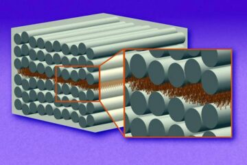
“Nanostitches” enable lighter and tougher composite materials
In research that may lead to next-generation airplanes and spacecraft, MIT engineers used carbon nanotubes to prevent cracking in multilayered composites. To save on fuel and reduce aircraft emissions, engineers…
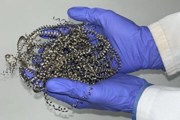
Trash to treasure
Researchers turn metal waste into catalyst for hydrogen. Scientists have found a way to transform metal waste into a highly efficient catalyst to make hydrogen from water, a discovery that…
Real-time detection of infectious disease viruses
… by searching for molecular fingerprinting. A research team consisting of Professor Kyoung-Duck Park and Taeyoung Moon and Huitae Joo, PhD candidates, from the Department of Physics at Pohang University…

