Tiny ’nanofingers’ to support sensors, other applications
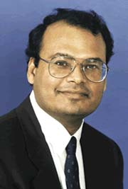
Sheikh Akbar
Future sensors may take the form of microscopic finger-like structures developed at Ohio State University.
Engineers here have found an easy way to carve the surface of inexpensive ceramic material into tiny filaments, creating a platform for devices that detect chemicals in the air. They could also be used to clean up toxic chemicals or gather solar energy, or to form fog-free or self-cleaning surfaces.
Each filament, or “nanofinger,” consists of a single crystal of the compound titanium oxide, and measures up to five micrometers long and at most 50 nanometers wide. A micrometer is one millionth of a meter, and a nanometer is one billionth of a meter.
The new process offers a simple chemical alternative to typical machine-based methods for carving ceramics, explained Sheikh Akbar, professor of materials science and engineering and founding director of the Center for Industrial Sensors and Measurements at Ohio State. Manufacturers often use diamond-edged rotary tools, lasers, or even ultrasound, because ceramics are hard and prone to chipping.
“Machining ceramics isn’t easy,” Akbar said. “This might be another way.” The patent-pending process is unique, he said, because it carves uniform filaments on a very small scale.
Materials science student Sehoon Yoo discovered the process and is developing it to earn his doctoral degree, with Akbar as his advisor. Kenneth Sandhage, formerly a professor at Ohio State and now at the Georgia Institute of Technology, is also advising Yoo.
Akbar described the process December 8 during the International Conference on Materials for Advanced Technologies meeting in Singapore.
The idea for the project came to Akbar when he attended a chemistry lecture in Japan in 1998. Researchers there had learned how to carve nanometer-sized honeycombs in ceramic. But because the procedure was very complicated, the speaker remarked that it had no practical commercial use.
“I thought, this is a great platform for chemical sensing,” Akbar said.
He then set Yoo to work to find a better process for carving honeycombs, and the student discovered how to carve nanofingers instead.
Yoo’s method involves baking the ceramic compound titanium dioxide at high heat inside a cloud of hydrogen gas. The hydrogen reacts with some of the oxygen in the material to create water, and heat binds the atoms of the ceramic together. What’s left is a very dense ceramic minus some oxygen atoms — its then simply titanium oxide — covered in a uniform array of nanofingers.
“We’re still not sure exactly how it works,” Yoo said. He suspects that somehow the chemical reaction frees atoms of titanium that normally remain bound in the material.
He’s tried the same experiment with other chemical elementsoxides — tin, cerium, and zirconium — to no avail, and will soon examine molybdenum and tungsten. But his work with titanium has advanced to the point that he can turn a penny-sized sample of the material into a rudimentary sensor that detects hydrogen.
When a hydrogen atom touches a finger, the finger absorbsreacts with it, and releases an electron. The electron travels down the finger to the base of the material, where the charge can be detected as a sensor signal.
The nanofingers provide a large surface area — good for capturing chemicals from the air, Akbar said.
That’s why the material would also be good for gathering light for electricity-generating solar cells. Another potential application is photocatalysis, in which light activates chemical reactions that clean contaminants from soil or water. The fingers could be coated with different chemicals for different functions, Akbar said.
“What’s really great about this process is that it involves no fancy techniques. All you need is a furnace and a cylinder of hydrogen,” he added.
Contact: Sheikh Akbar, (614) 292-6725; Akbar.1@osu.edu
Sehoon Yoo, (614) 292-7427; Yoo.89@osu.edu
Written by Pam Frost Gorder, (614) 292-9475; Gorder.1@osu.edu
Media Contact
More Information:
http://www.acs.ohio-state.edu/units/research/All latest news from the category: Materials Sciences
Materials management deals with the research, development, manufacturing and processing of raw and industrial materials. Key aspects here are biological and medical issues, which play an increasingly important role in this field.
innovations-report offers in-depth articles related to the development and application of materials and the structure and properties of new materials.
Newest articles
Silicon Carbide Innovation Alliance to drive industrial-scale semiconductor work
Known for its ability to withstand extreme environments and high voltages, silicon carbide (SiC) is a semiconducting material made up of silicon and carbon atoms arranged into crystals that is…
New SPECT/CT technique shows impressive biomarker identification
…offers increased access for prostate cancer patients. A novel SPECT/CT acquisition method can accurately detect radiopharmaceutical biodistribution in a convenient manner for prostate cancer patients, opening the door for more…
How 3D printers can give robots a soft touch
Soft skin coverings and touch sensors have emerged as a promising feature for robots that are both safer and more intuitive for human interaction, but they are expensive and difficult…


