Materials could make for super LEDs, solar cells, computer chips
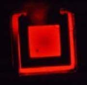
Engineers at Ohio State University have built bright light-emitting diodes (LEDs) on silicon substrates. One such LED is shown here. The new LEDs have a display quality comparable to that of traditional LEDs. Photo courtesy of Ohio State University.
Engineers at Ohio State University have overcome a major barrier in the manufacture of high quality light emitting devices and solar cell materials.
Steven Ringel, professor of electrical engineering, and his colleagues have created special hybrid materials that are virtually defect-free — an important first step for making ultra-efficient electronics in the future.
The same technology could also lead to faster, less expensive computer chips.
Ringel directs Ohio State’s Electronic Materials and Devices Laboratory, where he and his staff grow thin films of “III-V” semiconductors — materials made from elements such as gallium and arsenic, which reside in groups III and V of the chemical periodic table.
Because III-V materials absorb and emit light much more efficiently than silicon, these materials could bridge the gap between traditional silicon computer chips and light-related technologies, such as lasers, displays, and fiber optics.
Researchers have tried for years to combine III-V materials with silicon, but only with limited success. Now that Ringel has succeeded in producing the combination with record quality, he has set his sights on a larger goal.
“Ultimately, we’d like to develop materials that will let us integrate many different technologies on a single platform,” Ringel said.
Key to Ringel’s strategy is the idea of a “virtual substrate” — a generic chip-like surface that would be compatible with many different kinds of technologies, and could easily be tailored to suit different applications.
Ohio State graduate student Ojin Kwon reported the project’s latest results December 2 at the Materials Research Society meeting in Boston. Other coauthors include graduate student John Boeckl, also of Ohio State; and postdoctoral researcher Minjoo Lee, graduate student Arthur Pitera, and professor Eugene Fitzgerald, all of the Massachusetts Institute of Technology.
Ringel’s current materials design consists of a substrate of silicon topped with III-V materials such as gallium and arsenide, with hybrid silicon-germanium layers sandwiched in-between. The substrate is 0.7 millimeters thick, while the gallium arsenide layer is only 3 micrometers — millionths of a meter — thick.
Other labs have experimented with III-V materials grown on silicon, but none have been able to reduce defect levels below a critical level that would enable devices like light emitting diodes and solar cells to be achieved, Ringel said.
Defects occur when the thin layers of atoms in a film aren’t lined up properly. Small mismatches between layers rob the material of its ability to transmit electrical charge efficiently.
Ringel and his colleagues grew films of III-V semiconductors with a technique known as molecular beam epitaxy, in which evaporated molecules of a substance settle in thin layers on the surface of the silicon-germanium alloy. They then used techniques such as transmission electron microscopy to search for defects.
Defects are missing or misplaced atoms that trap electrons within the material, Ringel explained. That’s why engineers typically measure the quality of a solar cell material in terms of carrier lifetime — the length of time an electron can travel freely through a material without falling into a defect.
Other experimental III-V materials grown on silicon have achieved carrier lifetimes of about two nanoseconds, or two billionths of a second. Ringel’s materials have achieved carrier lifetimes in excess of 10 nanoseconds.
The engineers have crafted the III-V material into one-square-inch versions of solar cells in the laboratory, and achieved 17 percent efficiency at converting light to electricity. They have also built bright light-emitting diodes (LEDs) on silicon substrates that have a display quality comparable to that of traditional LEDs.
The next phase in this research will carry Ringel’s materials into space, as part of NASA’s Materials International Space Station Experiment (MISSE). An international partner spacecraft will deliver samples of the materials to the space station so they can be tested and possibly developed for use in future spacecraft.
This work was funded by the Army Research Office and the National Science Foundation.
Contact: Steven Ringel, (614) 292-6904; Ringel.1@osu.edu
Written by Pam Frost Gorder, (614) 292-9475; Gorder.1@osu.edu
Media Contact
More Information:
http://researchnews.osu.edu/archive/35led.htmAll latest news from the category: Materials Sciences
Materials management deals with the research, development, manufacturing and processing of raw and industrial materials. Key aspects here are biological and medical issues, which play an increasingly important role in this field.
innovations-report offers in-depth articles related to the development and application of materials and the structure and properties of new materials.


Newest articles
Machine learning algorithm reveals long-theorized glass phase in crystal
Scientists have found evidence of an elusive, glassy phase of matter that emerges when a crystal’s perfect internal pattern is disrupted. X-ray technology and machine learning converge to shed light…
Mapping plant functional diversity from space
HKU ecologists revolutionize ecosystem monitoring with novel field-satellite integration. An international team of researchers, led by Professor Jin WU from the School of Biological Sciences at The University of Hong…
Inverters with constant full load capability
…enable an increase in the performance of electric drives. Overheating components significantly limit the performance of drivetrains in electric vehicles. Inverters in particular are subject to a high thermal load,…

