NIST polishes method for creating tiny diamond machines
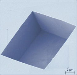
This colorized electron microscope image reveals the boxy shape of the pits the NIST team etched into the diamond surface, exhibiting their smooth vertical sidewalls and flat bottom. The pits were between 1 and 72 micrometers in size. Credit: NIST<br>
By combining their own observations with background gleaned from materials science, NIST semiconductor researchers have found a way to create unique features in diamond—potentially leading to improvements in nanometrology in short order, as it has allowed the team to make holes of precise shape in one of the hardest known substances. But beyond the creation of virtually indestructible nanorulers, the method could one day lead to the improvement of a class of electronic devices useful in cell phones, gyroscopes and medical implants.
Well known for making the hugely complex electronic microchips that run our laptops, the semiconductor industry has expanded its portfolio by fabricating tiny devices with moving parts. Constructed with substantially the same techniques as the electronic chips, these “micro-electromechanical systems,” or MEMS, are just a few micrometers in size. They can detect environmental changes such as heat, pressure and acceleration, potentially enabling them to form the basis of tiny sensors and actuators for a host of new devices. But designers must take care that tiny moving parts do not grind to a disastrous halt. One way to make the sliding parts last longer without breaking down is to make them from a tougher material than silicon.
“Diamond may be the ideal substance for MEMS devices,” says NIST's Craig McGray. “It can withstand extreme conditions, plus it's able to vibrate at the very high frequencies that new consumer electronics demand. But it's very hard, of course, and there hasn't been a way to engineer it very precisely at small scales. We think our method can accomplish that.”
The method uses a chemical etching process to create cavities in the diamond surface. The cubic shape of a diamond crystal can be sliced in several ways—a fact jewelers take advantage of when creating facets on gemstones. The speed of the etching process depends on the orientation of the slice, occurring at a far slower rate in the direction of the cube's “faces”—think of chopping the cube into smaller cubes—and these face planes can be used as a sort of boundary where etching can be made to stop when desired. In their initial experiments, the team created cavities ranging in width from 1 to 72 micrometers, each with smooth vertical sidewalls and a flat bottom.
“We'd like to figure out how to optimize control of this process next,” McGray says, “but some of the ways diamond behaved under the conditions we used were unexpected. We plan to explore some of these mysteries while we develop a prototype diamond MEMS device.”
* C.D. McGray, R.A. Allen, M. Cangemi and J. Geist. Rectangular scale-similar etch pits in monocrystalline diamond. Diamond and Related Materials. Available online 22 August 2011, ISSN 0925-9635, 10.1016/j.diamond.2011.08.007
Media Contact
More Information:
http://www.nist.govAll latest news from the category: Materials Sciences
Materials management deals with the research, development, manufacturing and processing of raw and industrial materials. Key aspects here are biological and medical issues, which play an increasingly important role in this field.
innovations-report offers in-depth articles related to the development and application of materials and the structure and properties of new materials.


Newest articles

Superradiant atoms could push the boundaries of how precisely time can be measured
Superradiant atoms can help us measure time more precisely than ever. In a new study, researchers from the University of Copenhagen present a new method for measuring the time interval,…

Ion thermoelectric conversion devices for near room temperature
The electrode sheet of the thermoelectric device consists of ionic hydrogel, which is sandwiched between the electrodes to form, and the Prussian blue on the electrode undergoes a redox reaction…

Zap Energy achieves 37-million-degree temperatures in a compact device
New publication reports record electron temperatures for a small-scale, sheared-flow-stabilized Z-pinch fusion device. In the nine decades since humans first produced fusion reactions, only a few fusion technologies have demonstrated…

