Materials for first optical fibers with high-speed electronic function are developed
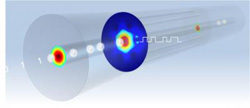
For the first time, researchers have developed crystalline materials that allow an optical fiber to have integrated, high-speed electronic functions. The potential applications of such optical fibers include improved telecommunications and other hybrid optical and electronic technologies, improved laser technology, and more-accurate remote-sensing devices. The international team, led by John Badding, a professor of chemistry at Penn State, will publish its findings in the journal Nature Photonics. The team built an optical fiber with a high-speed electronic junction -- the active boundary where all the electronic action takes place -- integrated adjacent to the light-guiding fiber core. Light pulses (white spheres) traveling down the fiber can be converted to electrical signals (square wave) inside the fiber by the junction. The potential applications of such optical fibers include improved telecommunications and other hybrid optical and electronic technologies and improved laser technology. Credit: John Badding lab, Penn State University<br>
The potential applications of such optical fibers include improved telecommunications and other hybrid optical and electronic technologies, improved laser technology, and more-accurate remote-sensing devices.
The research was initiated by Rongrui He, a postdoctoral researcher in the Department of Chemistry at Penn State University. The international team, led by John Badding, a professor of chemistry at Penn State, will publish its findings in the journal Nature Photonics.
Badding explained that one of the greatest current technological challenges is exchanging information between optics and electronics rapidly and efficiently. Existing technology has resulted in sometimes-clumsy ways of merging optical fibers with electronic chips — silicon-based integrated circuits that serve as the building blocks for most semiconductor electronic devices such as solar cells, light-emitting diodes (LEDs), computers, and cell phones. “The optical fiber is usually a passive medium that simply transports light, while the chip is the piece that performs the electrical part of the equation,” Badding said.
“For example, light is transmitted from London to New York via fiber-optic cables when two people set up a video call on their computers. But the computer screens and associated electronic devices have to take that light and convert it to an image, which is an electrical process. Light and electricity are working in concert in a process called an OEO conversion, or an optical-electrical-optical conversion.” Badding said that, ideally, rather than coupling the optical fiber to the chip, as is routine in existing technology, a “smart fiber” would have the electronic functions already built in.
The integration of optical fibers and chips is difficult for many reasons. First, fibers are round and cylindrical, while chips are flat, so simply shaping the connection between the two is a challenge. Another challenge is the alignment of pieces that are so small. “An optical fiber is 10 times smaller than the width of a human hair. On top of that, there are light-guiding pathways that are built onto chips that are even smaller than the fibers by as much as 100 times,” Badding said. “So imagine just trying to line those two devices up. That feat is a big challenge for today's technology.”
To address these challenges, the team members took a different approach. Rather than merge a flat chip with a round optical fiber, they found a way to build a new kind of optical fiber with its own integrated electronic component, thereby bypassing the need to integrate fiber-optics onto a chip. To do this, they used high-pressure chemistry techniques to deposit semiconducting materials directly, layer by layer, into tiny holes in optical fibers. “The big breakthrough here is that we don't need the whole chip as part of the finished product. We have managed to build the junction — the active boundary where all the electronic action takes place — right into the fiber,” said Pier J. A. Sazio of the University of Southampton in the United Kingdom and one of the team's leaders. “Moreover, while conventional chip fabrication requires multimillion-dollar clean-room facilities, our process can be performed with simple equipment that costs much less.”
Sazio added that one of the key goals of research in this field is to create a fast, all-fiber network. “If the signal never leaves the fiber, then it is a faster, cheaper, and more efficient technology,” said Sazio. “Moving technology off the chip and directly onto the fiber, which is the more-natural place for light, opens up the potential for embedded semiconductors to carry optoelectronic applications to the next level. At present, you still have electrical switching at both ends of the optical fiber. If we can actually generate signals inside a fiber, a whole range of optoelectronic applications becomes possible.”
The research also has many potential non-telecommunications applications. “For example, our work also represents a very different approach to fabricating semiconductor junctions that we are investigating for solar-cell applications,” said Badding.
In addition to Badding, Sazio, and He, other researchers who contributed to this study include Venkatraman Gopalan of Penn State, and Anna C. Peacock and Noel Healy of the Optoelectronics Research Centre in the United Kingdom.
The research was funded by the U.S. National Science Foundation and the Engineering and Physical Sciences Research Council of the United Kingdom.
[ Katrina Voss ]
CONTACTS
John Badding: 814-777-3054 (mobile), jbadding@pearl.chem.psu.edu
Pier J. A. Sazio: 44-23-8059-3144, pjas@orc.soton.ac.uk
Barbara Kennedy (PIO): 814-863-4682, science@psu.edu
Media Contact
More Information:
http://www.psu.eduAll latest news from the category: Materials Sciences
Materials management deals with the research, development, manufacturing and processing of raw and industrial materials. Key aspects here are biological and medical issues, which play an increasingly important role in this field.
innovations-report offers in-depth articles related to the development and application of materials and the structure and properties of new materials.


Newest articles

Bringing bio-inspired robots to life
Nebraska researcher Eric Markvicka gets NSF CAREER Award to pursue manufacture of novel materials for soft robotics and stretchable electronics. Engineers are increasingly eager to develop robots that mimic the…

Bella moths use poison to attract mates
Scientists are closer to finding out how. Pyrrolizidine alkaloids are as bitter and toxic as they are hard to pronounce. They’re produced by several different types of plants and are…

AI tool creates ‘synthetic’ images of cells
…for enhanced microscopy analysis. Observing individual cells through microscopes can reveal a range of important cell biological phenomena that frequently play a role in human diseases, but the process of…

