Laser source for biosensors
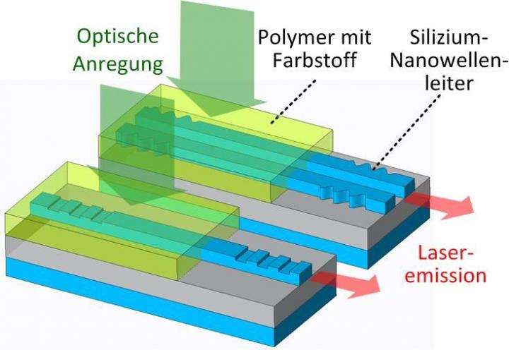
Organic laser on a silicon photonic chip: Optical excitation from above generates laser light in the waveguide. Graphics: KIT
In the area of nano photonics, scientists for the first time succeeded in integrating a laser with an organic gain medium on a silicon photonic chip. This approach is of enormous potential for low-cost biosensors that might be used for near-patient diagnosis once and without any sterilization expenditure similar to today's strips for measuring blood sugar. The researchers now present the new laser in Nature Communications: DOI: 10.1038/ncomms10864
This is the first time organic lasers were integrated on a single silicon photonic chip, Christian Koos, researcher of KIT's Institute of Photonics and Quantum Electronics (IPQ) and Institute of Microstructure Technology (IMT), reports. “The main advantage of the lasers consists in the fact that production of large series is associated with low costs. In the long term, manufacture at a price of some cents per laser might be feasible.”
One of the major challenges associated with the fabrication of optical microchips consists in integrating a number of different components on one substrate at low cost. For some years now, it has been possible to produce optical components from silicon.
This so-called silicon photonics uses highly developed nanotechnological fabrication processes of microelectronics and allows for the inexpensive production of large numbers of high-performance photonic components. Such components of fractions of a micrometer in size can contribute to making information technology more energy-efficient and are highly suited for compact biosensors.
The problem of integrating light sources on the chip, however, still remained unsolved, as the silicon semiconductor is hardly suited as a light emitter due to its electronic structure. During electron transfer between energetically different states, the energy is preferably released in the form of heat rather than light.
Researchers of KIT have now developed a new class of lasers in the infrared range. For this purpose, they combine silicon nano waveguides with a polymer doped with an organic dye. The energy to operate this “organic” laser is supplied from above, vertically to the chip surface, by a pulsed light source. The laser light produced is directly coupled into a silicon nano waveguide.
The researchers succeeded in generating pulsed laser radiation with a wavelength of 1310 nm and a peak power of more than 1 Watt on one chip. The new infrared lasers are presented in the Nature Communications journal. By the use of various dyes and laser resonators, the wavelength of laser radiation can be varied over a wide range.
Dietmar Korn, Matthias Lauermann, Sebastian Koeber, Patrick Appel, Luca Alloatti, Robert Palmer, Pieter Dumon, Wolfgang Freude, Juerg Leuthold & Christian Koos: Lasing in silicon-organic hybrid waveguides. Nature Communications, 2016. DOI: 10.1038/ncomms10864
For further information, please contact:
Kosta Schinarakis
PKM — Science Scout
Phone: 49-721-608-41956
Fax: 49-721-608-43658
E-mail: schinarakis@kit.edu
Karlsruhe Institute of Technology (KIT) pools its three core tasks of research, higher education, and innovation in a mission. With about 9,300 employees and 25,000 students, KIT is one of the big institutions of research and higher education in natural sciences and engineering in Europe.
KIT — The Research University in the Helmholtz Association
Since 2010, the KIT has been certified as a family-friendly university.
This press release is available on the internet at http://www.
The photo of printing quality may be downloaded under http://www.
Media Contact
All latest news from the category: Materials Sciences
Materials management deals with the research, development, manufacturing and processing of raw and industrial materials. Key aspects here are biological and medical issues, which play an increasingly important role in this field.
innovations-report offers in-depth articles related to the development and application of materials and the structure and properties of new materials.


Newest articles

Silicon Carbide Innovation Alliance to drive industrial-scale semiconductor work
Known for its ability to withstand extreme environments and high voltages, silicon carbide (SiC) is a semiconducting material made up of silicon and carbon atoms arranged into crystals that is…

New SPECT/CT technique shows impressive biomarker identification
…offers increased access for prostate cancer patients. A novel SPECT/CT acquisition method can accurately detect radiopharmaceutical biodistribution in a convenient manner for prostate cancer patients, opening the door for more…

How 3D printers can give robots a soft touch
Soft skin coverings and touch sensors have emerged as a promising feature for robots that are both safer and more intuitive for human interaction, but they are expensive and difficult…

