International researchers discuss at INM how the mechanics of materials changes with size
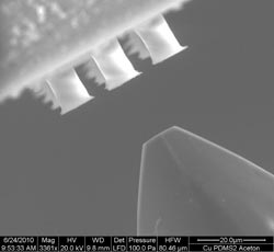
PDMS Pillars with Nanoindenter<br>INM<br>
Thus, the wire remains intact even when bent. Only when the copper grains are smaller than one thousandth of a millimeter, the properties change and therefore the metal's behavior:
It becomes harder and breaks faster. During the international workshop Nanobruecken II at INM – Leibniz Institute for New Materials on 22 and 23 March 2012, materials researchers from Europe discussed why such mechanical properties of a material change in smallest dimensions.
“We know that materials in size ranges under one thousandth of a millimeter behave mechanically in a different way from larger units”, says Roland Bennewitz, head of the program division “Nanotribology”. “It is not completely understood yet, why and how materials change their properties in smaller units. If our measurements allow us to explain the determining factors behind it, we will be able to tailor the mechanical behavior of materials in the future”, explained the physicist. A certain hardness, viscosity, deformability and even combinations of these properties could then be precisely tailored. New concepts for hardened metal surfaces or sliding rubber seals are imaginable in the future.
In order to understand the phenomena behind it, the researchers use special analytical methods. The so-called nanoindenter has a sharp tip, which is pressed into the surface of a material sample, examining its deformability. At INM, the researchers are able to produce samples with microscopic dimensions. By the so-called “ion-etching” very small pillars with different diameters are produced, which are scanned by a sharp tip.
Important parameters are the tip's depth of indentation, the energy needed, or the way the pillars are crushed during the scanning. The whole process is done in a dimension of only a few millionths of millimeters. “For the measurements, we use a special nanoindenter developed by Hysitron, whose measuring possibilities were tailored especially to our needs”, the materials expert explains. Usually, hard probes, i.e. metals, ceramic or even nacre, can be examined with such equipment. But it is no problem to also examine smooth probes, such as plastics, with the specially developed equipment.
For the scientific discussions, INM invited international researchers with their special knowhow. 60 researchers from Europe took part in the two-day congress Nanobruecken II. Nanobruecken is taking place at INM for the second time. In workshops, the company Hysitron presents technical innovations of their nanoindenters.
Contact:
Professor Dr. Roland Bennewitz
INM – Leibniz-Institut für Neue Materialien gGmbH
Programmbereichsleiter Nanotribologie
Tel.: +49 (0)681-9300-213
E-mail: roland.bennewitz@inm-gmbh.de
INM is focused on the research and development of materials – for today, tomorrow and the future. Chemists, physicists, biologists, materials and engineering scientists shape the work at INM. From molecule to pilot production, they follow three essential questions: Which material properties are new, how can they be investigated and how can they be used for industrial and true-to-life applications in the future?
INM – Leibniz Institute for New Materials, situated in Saarbrücken/Germany, is an internationally leading centre for materials research. It is a scientific partner to national and international institutes and a provider of research and development for companies throughout the world. INM is an institute of the Scientific Association Gottfried Wilhelm Leibniz and employs around 190 collaborators. Its main research fields are Chemical Nanotechnology, Interface Materials, and Materials in Biology.
Media Contact
All latest news from the category: Materials Sciences
Materials management deals with the research, development, manufacturing and processing of raw and industrial materials. Key aspects here are biological and medical issues, which play an increasingly important role in this field.
innovations-report offers in-depth articles related to the development and application of materials and the structure and properties of new materials.


Newest articles

Silicon Carbide Innovation Alliance to drive industrial-scale semiconductor work
Known for its ability to withstand extreme environments and high voltages, silicon carbide (SiC) is a semiconducting material made up of silicon and carbon atoms arranged into crystals that is…

New SPECT/CT technique shows impressive biomarker identification
…offers increased access for prostate cancer patients. A novel SPECT/CT acquisition method can accurately detect radiopharmaceutical biodistribution in a convenient manner for prostate cancer patients, opening the door for more…

How 3D printers can give robots a soft touch
Soft skin coverings and touch sensors have emerged as a promising feature for robots that are both safer and more intuitive for human interaction, but they are expensive and difficult…

