Infrared light visualizes nanoscale strain fields
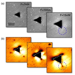
Infrared visualization of nanocrack evolution. a) Topography of triangular indents (depressions) at the surface of a SiC crystal. Indentation was performed by pressing a sharp diamond tip into the crystal surface. With increasing force F, the depression becomes larger and deeper. b) The infrared near-field images recorded at about 10 µm wavelength clearly show the regions around the indent where the crystal lattice is compressed (bright) or stretched (dark). Because of the exceptional high spatial resolution, the images reveal the onset and formation of nanoscale cracks (marked by dashed blue circlse) when the indentation force is increased. Copyright: Andreas Huber, Max Planck Institute of Biochemistry, Martinsried<br>
The method, which is based on near-field microscopy, opens new avenues for analyzing mechanical properties of high-performance materials or for contact-free mapping of local conductivity in strain-engineered electronic devices (Nature Nanotechnology, advanced online publication, 11 Jan. 2009).
Visualizing strain at length scales below 100 nm is a key requirement in modern metrology because strain determines the mechanical and electrical properties of high-performance ceramics or modern electronic devices, respectively. The non-invasive mapping of strain with nanoscale spatial resolution, however, is still a challenge.
A promising route for highly sensitive and non-invasive mapping of nanoscale material properties is scattering-type Scanning Near-field Optical Microscopy (s-SNOM). Part of the team had pioneered this technique over the last decade, enabling chemical recognition of nanostructures and mapping of local conductivity in industrial semiconductor nanodevices. The technique makes use of extreme light concentration at the sharp tip of an Atomic Force Microscope (AFM), yielding nanoscale resolved images at visible, infrared and terahertz frequencies. The s-SNOM thus breaks the diffraction barrier throughout the electromagnetic spectrum and with its 20 nm resolving power matches the needs of modern nanoscience and technology.
Now, the research team has provided first experimental evidence that the microscopy technique is capable of mapping local strain and cracks of nanoscale dimensions. This was demonstrated by pressing a sharp diamond tip into the surface of a Silicon Carbide crystal. With the near-field microscope the researchers were able to visualize the nanoscopic strain field around the depression and the generation of nanocracks (see Figure). “Compared to other methods such as electron microscopy, our technique offers the advantage of non-invasive imaging without the need of special sample preparation” says Andreas Huber who performed the experiments within his Ph.D. project. “Specific applications of technological interest could be the detection of nanocracks before they reach critical dimensions, e.g. in ceramics or Micro-Electro-Mechanical Systems (MEMS), and the study of crack propagation”, says Alexander Ziegler.
The researchers also demonstrated that s-SNOM offers the intriguing possibility of mapping free-carrier properties such as density and mobility in strained silicon. By controlled straining of silicon, the properties of the free carriers can be designed, which is essential to further shrink and speed-up future computer chips. For both development and quality control, the quantitative and reliable mapping of the carrier mobility is strongly demanded but hitherto no tool has been available. “Our results thus promise interesting applications of s-SNOM in semiconductor science and technology such as the quantitative analysis of the local carrier properties in strain-engineered electronic nanodevices” says Rainer Hillenbrand, leader of the Nano-Photonics Group at MPI and the Nanooptics Laboratory at nanoGUNE.
Original publication:
A. J. Huber, A. Ziegler, T. Köck, and R. Hillenbrand, Infrared nanoscopy of strained semiconductors, Nat. Nanotech., advanced online publication, 11. Jan. 2009, DOI 10.1038/NNANO.2008.399.
Contact:
Dr. Rainer Hillenbrand
Nanooptics Laboratory
CIC nanoGUNE Consolider
20009 Donostia – San Sebastian, Spain
phone: +34 943 574 007
r.hillenbrand@nanogune.eu
and
Nano-Photonics Group
Max-Planck-Institut für Biochemie
82152 Martinsried, Germany
Media Contact
All latest news from the category: Materials Sciences
Materials management deals with the research, development, manufacturing and processing of raw and industrial materials. Key aspects here are biological and medical issues, which play an increasingly important role in this field.
innovations-report offers in-depth articles related to the development and application of materials and the structure and properties of new materials.


Newest articles

Superradiant atoms could push the boundaries of how precisely time can be measured
Superradiant atoms can help us measure time more precisely than ever. In a new study, researchers from the University of Copenhagen present a new method for measuring the time interval,…

Ion thermoelectric conversion devices for near room temperature
The electrode sheet of the thermoelectric device consists of ionic hydrogel, which is sandwiched between the electrodes to form, and the Prussian blue on the electrode undergoes a redox reaction…

Zap Energy achieves 37-million-degree temperatures in a compact device
New publication reports record electron temperatures for a small-scale, sheared-flow-stabilized Z-pinch fusion device. In the nine decades since humans first produced fusion reactions, only a few fusion technologies have demonstrated…

