Hybrid nanostructures: Getting to the core
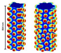
Simulations showing the potential growth of quantum dots on the ridges and facets of nanowires with square (left) and hexagonal cores (right). <br><br>Reproduced, with permission, from Ref. 1 © 2013 American Chemical Society<br>
Material scientists expect the new multifunctional properties of hybrid nanostructures will transform the development of high-performance devices, including batteries, high-sensitivity sensors and solar cells.
These self-assembling nanostructures are typically generated by depositing ultrasmall objects with different properties on the surfaces of tiny semiconducting wires. However, the factors that govern their formation remain elusive, making these structures difficult to control and design.
To fill this gap, Bharathi Srinivasan and co-workers from the A*STAR Institute of High Performance Computing have developed a computational approach that sheds light on the self-assembly of these nanostructures on multi-sided, or polygonal, nanowires. They first identified how different nanostructure patterns grow on nanowires by conducting energy calculations in a theoretical analysis before analyzing these patterns by performing numerical simulations.
Srinivasan’s team designed two- and three-dimensional (2D and 3D) models of nanowires with a square, hexagonal or octagonal core surrounded by various shell configurations. Analysis of the energy profiles of these configurations showed that the researchers could control shell morphology by changing the core size. The theoretical analysis also revealed the transitions between these different configurations — a valuable insight into the self-assembly mechanism.
For the numerical simulation, the researchers constructed a ‘phase-field’ model, which mathematically defined the phase transitions of the shell material. This allowed them to simulate the self-assembly process of the nanostructures on the nanowires after depositing the ‘seed’ in the form of ‘quantum dots’, which are miniature semiconductors. The equations used in the simulation describe both the thermodynamics and the kinetics of self-assembly, Srinivasan notes.
Both the 2D and 3D simulations showed that the deposited shells underwent morphological transformations that mirrored the energy calculations. At the initial deposition stage — the lowest size range — the shells consisted of perfect cylinders in the 2D model, and they formed ultrasmall rings, or ‘nanorings’, stacked along the vertical direction of the nanowire, in the 3D model.
As the core expanded, the 2D models indicated that the shells could break into smaller wires. For the intermediate-sized cores, each wire sat on the sides of the core. For the largest-sized cores, they sat on the corners. In the 3D simulations, the nanorings divided into quantum dots that materialized into columns on the nanowire facets and migrated towards the ridges upon further growth (see image). Simulations of heat treatment yielded the same configurations as those during growth.
“Our future work [will be] to understand the growth of different hybrid nanostructures, including quantum dots on shells, nanorings and other quantum dots,” says Srinivasan.
The A*STAR-affiliated researchers contributing to this research are from the Institute of High Performance Computing
Journal information
Lu, L.-X., Bharathi M. S. & Zhang, Y.-W. Self-assembly of ordered epitaxial nanostructures on polygonal nanowires. Nano Letters 13, 538–542 (2013).
Media Contact
More Information:
http://www.research.a-star.edu.sg/research/6690All latest news from the category: Materials Sciences
Materials management deals with the research, development, manufacturing and processing of raw and industrial materials. Key aspects here are biological and medical issues, which play an increasingly important role in this field.
innovations-report offers in-depth articles related to the development and application of materials and the structure and properties of new materials.


Newest articles

Silicon Carbide Innovation Alliance to drive industrial-scale semiconductor work
Known for its ability to withstand extreme environments and high voltages, silicon carbide (SiC) is a semiconducting material made up of silicon and carbon atoms arranged into crystals that is…

New SPECT/CT technique shows impressive biomarker identification
…offers increased access for prostate cancer patients. A novel SPECT/CT acquisition method can accurately detect radiopharmaceutical biodistribution in a convenient manner for prostate cancer patients, opening the door for more…

How 3D printers can give robots a soft touch
Soft skin coverings and touch sensors have emerged as a promising feature for robots that are both safer and more intuitive for human interaction, but they are expensive and difficult…

