Graphene on its way to conquer Silicon Valley
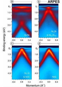
The above images were taken with the spectroscopy method ARPES while NiSi was formed under the graphene layer. In the final image (d) scientists can identify a particular spectrum (the linear Dirac-like spectrum of grapheme electrons) indicating that the graphene interacts only weakly with the metal silicides and therefore preserves its unique properties.(Copyright: Vilkov et al., Sci. Rep. 2013, DOI: 10.1038/srep02168) <br>
Researchers of the Electronic Properties of Materials Group at the University of Vienna have now paved the way for the integration of graphene into the current silicide based technology. They have published their results in the new open access journal of the Nature Publishing group, Scientific Reports.
The unique properties of graphene such as its incredible strength and, at the same time, its little weight have raised high expectations in modern material science. Graphene, a two-dimensional crystal of carbon atoms packed in a honeycomb structure, has been in the focus of intensive research which led to a Nobel Prize of Physics in 2010. One major challenge is to successfully integrate graphene into the established metal-silicide technology. Scientists from the University of Vienna and their co-workers from research institutes in Germany and Russia have succeeded in fabricating a novel structure of high-quality metal silicides all nicely covered and protected underneath a graphene layer. These two-dimensional sheets are as thin as single atoms.
Following Einstein's footsteps
In order to uncover the basic properties of the new structure the scientists need to resort to powerful measurement techniques based on one of Einstein’s brilliant discoveries – the photoelectric effect. When a light particle interacts with a material it can transfer all its energy to an electron inside that material. If the energy of the light is sufficiently large, the electron acquires enough energy to escape from the material. Angle-resolved photoemission spectroscopy (ARPES) enables the scientists to extract valuable information on the electronic properties of the material by determining the angle under which the electrons escape from the material. “Single-atom thick layers and hybrid materials made thereof allow us to study a wealth of novel electronic phenomena and continue to fascinate the community of material scientists. The ARPES method plays a key role in these endeavours”, say Alexander Grueneis and Nikolay Verbitskiy, members of the Electronic Properties of Materials Group at the University of Vienna and co-authors of the study.
Graphene keeping its head up high
The graphene-capped silicides under investigation are reliably protected against oxidation and can cover a wide range of electronic materials and device applications. Most importantly, the graphene layer itself barely interacts with the silicides underneath and the unique properties of graphene are widely preserved. The work of the research team, therefore, promises a clever way to incorporate graphene with existing metal silicide technology which finds a wide range of applications in semiconductor devices, spintronics, photovoltaics and thermoelectrics.
The work on graphene related materials is financed by a Marie Curie fellowship of the European commission and an APART fellowship of the Austrian Academy of Sciences.
Original publication:
“Controlled assembly of graphene-capped nickel, cobalt and iron silicides”:
O. Vilkov, A. Fedorov, D. Usachov, L. V. Yashina, A. Generalov, K. Borygina, N. I. Verbitskiy, A. Grueneis, and D. V. Vyalikh Scientific Reports, July 9, 2013,
DOI: 10.1038/srep02168
Scientific Contact:
Dr. Alexander Grueneis
Electronic Properties of Materials
Faculty of Physics, University of Vienna
Boltzmanngasse 5, 1090 Vienna
M +43-664-602 77-513 72
alexander.grueneis@univie.ac.at
http://homepage.univie.ac.at/alexander.grueneis/highlights.html
Media Contact
More Information:
http://www.univie.ac.atAll latest news from the category: Materials Sciences
Materials management deals with the research, development, manufacturing and processing of raw and industrial materials. Key aspects here are biological and medical issues, which play an increasingly important role in this field.
innovations-report offers in-depth articles related to the development and application of materials and the structure and properties of new materials.


Newest articles

Silicon Carbide Innovation Alliance to drive industrial-scale semiconductor work
Known for its ability to withstand extreme environments and high voltages, silicon carbide (SiC) is a semiconducting material made up of silicon and carbon atoms arranged into crystals that is…

New SPECT/CT technique shows impressive biomarker identification
…offers increased access for prostate cancer patients. A novel SPECT/CT acquisition method can accurately detect radiopharmaceutical biodistribution in a convenient manner for prostate cancer patients, opening the door for more…

How 3D printers can give robots a soft touch
Soft skin coverings and touch sensors have emerged as a promising feature for robots that are both safer and more intuitive for human interaction, but they are expensive and difficult…

