Ferroelectricity on the Nanoscale
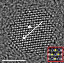
Atomic-resolution images of germanium telluride nanoparticles from Berkeley Lab’s TEAM I electron microscope, and electron holographic images of barium titanate nanoparticles (below) from BNL yielded the first detailed experimental information on ferroelectric order at the nanoscale.<br>
Promising news for those who relish the prospects of a one-inch chip storing multiple terabytes of data, some clarity has been brought to the here-to-fore confusing physics of ferroelectric nanomaterials.
A multi-institutional team of researchers, led by scientists at the U.S. Department of Energy (DOE)’s Lawrence Berkeley National Laboratory (Berkeley Lab) has provided the first atomic-scale insights into the ferroelectric properties of nanocrystals. This information will be critical for development of the next generation of nonvolatile data storage devices.
Working with the world’s most powerful transmission electron microscope, the researchers mapped the ferroelectric structural distortions in nanocrystals of germanium telluride, a semiconductor, and barium titanate, an insulator. This data was then combined with data from electron holographic polarization imaging to yield detailed information on the polarization structures and scaling limits of ferroelectric order on the nanoscale.
“As we scale down our device technology from the microscale to the nanoscale, we need a better understanding of how critical material properties, such as ferroelectric behavior, are impacted,” says Paul Alivisatos, director of Berkeley Lab and one of the principal investigators in this research. “Our results provide a pathway to unraveling the fundamental physics of nanoscale ferroelectricity at the smallest possible size scales.”
Alivisatos, who is also the Larry and Diane Bock Professor of Nanotechnology at the University of California (UC) Berkeley, is a corresponding author of a paper describing this work in the journal Nature Materials titled “Ferroelectric order in individual nanometrescale Crystals.” The other corresponding author is Ramamoorthy Ramesh, a senior scientist with Berkeley Lab’s Materials Sciences Division and the Plato Malozemoff Professor of Materials Science and Physics for UC Berkeley.
Ferroelectricity is the property by which materials can be electrically polarized, meaning they will be oriented in favor of either a positive or negative electrical charge. This polarization can be flipped with the application of an external electrical field, a property that could be exploited for nonvolatile data storage, similar to the use of ferromagnetic materials today but using much smaller, far more densely packed devices.
“Although much progress has been made towards understanding nanoscale photophysical magnetic and other functional properties, understanding the basic physics of ferroelectric nanomaterials remains far less advanced,” says co-principal investigator Ramesh, who attributes contradicting reports on nanoscale ferroelectricity in part to the lack of high-quality, nanocrystals of ferroelectric materials that feature well-defined sizes, shapes and surfaces.
“Another problem has been the reliance on ensemble measurements rather than single particle techniques,” he says. “Statistical-average measurement techniques tend to obscure the physical mechanisms responsible for profound changes in ferroelectric behavior within individual nanocrystals.”
The Berkeley Lab-led research team was able to map ferroelectric structural distortions within individual nanocrystals thanks to the unprecedented capabilities of TEAM I, which is housed at Berkeley Lab’s National Center for Electron Microscopy (NCEM). TEAM stands for “Transmission Electron Aberration-corrected Microscope.” TEAM I can resolve images of structures with dimensions as small as one half‑angstrom – less than the diameter of a single hydrogen atom.
The maps produced at TEAM I of ferroelectric distortion patterns within the highly conducting germanium telluride nanocrystals were then compared with electron holography studies of insulating nanocubes of barium titanate, which were carried out by collaborators at Brookhaven National Laboratory (BNL).
“Electron holography is an interferometry technique using coherent electron waves,” said BNL physicist and co-author of the Nature Materials paper Myung-Geun Han. “Firing focused electron waves through the ferroelectric sample creates what’s called a phase-shift, or an interference pattern that reveals details of the targeted structure. This produces an electron hologram, which we can use to directly see local electric fields of individual ferroelectric nanoparticles.”
These combined studies enabled the independent examination of depolarizing field and surface structure influences and thereby enabled the research team to identify the fundamental factors governing the nature of the ferroelectric polarized state at finite dimensions. The results indicate that a monodomain ferroelectric state with linearly ordered polarization remains stable in these nanocrystals down to dimensions of less than 10 nanometers. Also, room-temperature polarization flipping was demonstrated down to dimensions of about five nanometers. Below this threshold, ferroelectric behavior disappeared. This indicates that five nanometers is likely a size limit for data storage applications, the authors state.
“We also showed that ferroelectric coherence is facilitated in part by control of particle morphology, which along with electrostatic boundary conditions is found to determine the spatial extent of cooperative ferroelectric distortions,” Ramesh says. “Taken together, our results provide a glimpse of the structural and electrical manifestations of ferroelectricity down to its ultimate limits.”
Also co-authoring the Nature Materials paper in addition to Alivisatos, Ramesh and Han were Mark Polking, Amin Yourdkhani, Valeri Petkov, Christian Kisielowski, Vyacheslav Volkov, Yimei Zhu and Gabriel Caruntu.
This research was supported by the DOE Office of Science.
Lawrence Berkeley National Laboratory addresses the world’s most urgent scientific challenges by advancing sustainable energy, protecting human health, creating new materials, and revealing the origin and fate of the universe. Founded in 1931, Berkeley Lab’s scientific expertise has been recognized with 13 Nobel prizes. The University of California manages Berkeley Lab for the U.S. Department of Energy’s Office of Science. For more, visit www.lbl.gov.
One of ten national laboratories overseen and primarily funded by the Office of Science of the U.S. Department of Energy (DOE), Brookhaven National Laboratory conducts research in the physical, biomedical, and environmental sciences, as well as in energy technologies and national security. Brookhaven Lab also builds and operates major scientific facilities available to university, industry and government researchers. Brookhaven is operated and managed for DOE’s Office of Science by Brookhaven Science Associates, a limited-liability company founded by the Research Foundation for the State University of New York on behalf of Stony Brook University, the largest academic user of Laboratory facilities, and Battelle, a nonprofit, applied science and technology organization. Visit Brookhaven Lab’s electronic newsroom for links, news archives, graphics, and more at http://www.bnl.gov/newsroom, or follow Brookhaven Lab on Twitter, http://twitter.com/BrookhavenLab.
DOE’s Office of Science is the single largest supporter of basic research in the physical sciences in the United States, and is working to address some of the most pressing challenges of our time. For more information, please visit science.energy.gov.
Additional Information
For more information on the research of Ramamoorthy Ramesh, visit his Website at http://www.lbl.gov/msd/investigators/investigators_all/ramesh_investigator.html
For more information on the research of Paul Alivisatos visit his Website at http://www.cchem.berkeley.edu/pagrp/
For more about the National Center for Electron Microscopy and TEAM I visit the Website at http://ncem.lbl.gov/
Media Contact
All latest news from the category: Materials Sciences
Materials management deals with the research, development, manufacturing and processing of raw and industrial materials. Key aspects here are biological and medical issues, which play an increasingly important role in this field.
innovations-report offers in-depth articles related to the development and application of materials and the structure and properties of new materials.


Newest articles

Silicon Carbide Innovation Alliance to drive industrial-scale semiconductor work
Known for its ability to withstand extreme environments and high voltages, silicon carbide (SiC) is a semiconducting material made up of silicon and carbon atoms arranged into crystals that is…

New SPECT/CT technique shows impressive biomarker identification
…offers increased access for prostate cancer patients. A novel SPECT/CT acquisition method can accurately detect radiopharmaceutical biodistribution in a convenient manner for prostate cancer patients, opening the door for more…

How 3D printers can give robots a soft touch
Soft skin coverings and touch sensors have emerged as a promising feature for robots that are both safer and more intuitive for human interaction, but they are expensive and difficult…

