Crystal unclear: Why might this uncanny crystal change laser design?
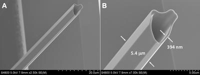
These potassium diphosphate (KDP) crystals, which self-assemble in solution as hollow hexagonal rods, could find use in laser technology, particularly for fiber-optic communications. The scanning-electron image at right shows a crystal at higher resolution with scale added. Credit: L. Deng / NIST
The findings, published today in Science Advances, suggest that the relatively large crystals used to change several properties of light in lasers – changes that are crucial for making lasers into practical tools – might be created by stacking up far smaller, rod-shaped microcrystals that can be grown easily and cheaply.
So far, the team's microcrystals outperform conventional crystals in some ways, suggesting that harnessing them could signal the end of a long search for a fast, economical way to develop large crystals that would otherwise be prohibitively expensive and time-consuming to create. But the microcrystals also challenge conventional scientific theory as to why they perform as they do.
The color you see in a laser's light is often different than the one it initially generates. Many lasers create infrared light, which then passes through a crystal converting its energy – and therefore its wavelength – to light of a visible color like green or blue.
Frequently, that crystal is made of potassium diphosphate (KDP), a common material that has properties that make it invaluable: Not only can a KDP crystal alter the light's color, but it also can act as a switch that changes the light's polarization (the direction in which its electric field vibrates) or prevent it from passing through the crystal until just the right moment. The data carried by laser light through fiber-optic cables depends on the light's polarization, and many applications depend on a laser pulse's timing.
Small KDP crystals are easy to make, and these find use in pocket laser pointers and telecommunications systems alike. But for higher-energy applications, scientists have searched for decades for a way to make large, high-quality crystals that can survive repeated exposure to intense laser pulses, but a solution has remained elusive.
The team has found useful results by growing KDP crystals in solution. These crystals take the form of hexagonal-shaped hollow tubes and long rods just a few micrometers wide. Individually, these KDP microcrystals have an energy-conversion efficiency surpassing even the best KDP crystals under the same conditions, raising the possibility of directly growing crystals for use in telecommunications.
The team also suggests the rods could be stacked up like firewood, building a larger piece out of billions of the tiny filaments. Before they are stacked together they could be coated by a thin layer of conductive material that carries heat away, rendering them capable of handling repeated pulses of high-intensity laser light – potentially broadening their application range if a way can be found to stack them.
The mystery is why the microcrystals perform as they do. Basic physics says they shouldn't.
Conventional physics models indicate that an optical medium like a crystal must not be symmetric about its center if it is to convert energy efficiently, yet these microcrystals appear to break this rule.
“We've spoken to a number of experts in different fields worldwide, and none of them can explain it,” says NIST physicist Lu Deng. “Currently no theory can explain the initial growth mechanism of this exotic crystal. It's challenging our current understanding in fields from crystallography to condensed matter physics.”
While theory catches up with data, Deng said the team is concentrating on the engineering challenges of growing stackable microcrystal rods.
“We can grow more than 1,000 microstructures every 10 minutes or so on a single glass slide, so growing a large amount is not a problem,” he said. “What we need to figure out is how to grow a large fraction of them with nearly uniform cross-sections since that will be important in the final assembly stage.”
Media Contact
All latest news from the category: Materials Sciences
Materials management deals with the research, development, manufacturing and processing of raw and industrial materials. Key aspects here are biological and medical issues, which play an increasingly important role in this field.
innovations-report offers in-depth articles related to the development and application of materials and the structure and properties of new materials.


Newest articles

Superradiant atoms could push the boundaries of how precisely time can be measured
Superradiant atoms can help us measure time more precisely than ever. In a new study, researchers from the University of Copenhagen present a new method for measuring the time interval,…

Ion thermoelectric conversion devices for near room temperature
The electrode sheet of the thermoelectric device consists of ionic hydrogel, which is sandwiched between the electrodes to form, and the Prussian blue on the electrode undergoes a redox reaction…

Zap Energy achieves 37-million-degree temperatures in a compact device
New publication reports record electron temperatures for a small-scale, sheared-flow-stabilized Z-pinch fusion device. In the nine decades since humans first produced fusion reactions, only a few fusion technologies have demonstrated…

